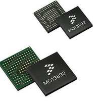
MC13892JVL Freescale Semiconductor, MC13892JVL Datasheet - Page 103

MC13892JVL
Manufacturer Part Number
MC13892JVL
Description
IC PMU I.MX51/37/35/27 186MAPBGA
Manufacturer
Freescale Semiconductor
Datasheets
1.MC13892AJVLR2.pdf
(156 pages)
2.MC13892AJVLR2.pdf
(2 pages)
3.MC13892AJVLR2.pdf
(16 pages)
4.MC13892JVL.pdf
(161 pages)
Specifications of MC13892JVL
Applications
Battery Management, Display (LED Drivers), Handheld/Mobile Devices, Power Supply
Operating Temperature
-40°C ~ 85°C
Mounting Type
Surface Mount
Package / Case
186-LFBGA
Output Current
65 mA
Output Voltage
1.5 V
Operating Temperature (max)
85C
Operating Temperature (min)
-40C
Mounting
Surface Mount
Package Type
BGA
Case Length
12mm
Screening Level
Industrial
Lead Free Status / RoHS Status
Lead free / RoHS Compliant
Current - Supply
-
Voltage - Supply
-
Lead Free Status / Rohs Status
Lead free / RoHS Compliant
Available stocks
Company
Part Number
Manufacturer
Quantity
Price
Company:
Part Number:
MC13892JVL
Manufacturer:
DALSA
Quantity:
4
Company:
Part Number:
MC13892JVL
Manufacturer:
Freescale Semiconductor
Quantity:
10 000
Part Number:
MC13892JVL
Manufacturer:
FREESCALE
Quantity:
20 000
Company:
Part Number:
MC13892JVLR2
Manufacturer:
Freescale Semiconductor
Quantity:
10 000
Table 90. Battery Removal Detect Specification
CHANNEL 5 ADIN5 AND BATTERY THERMISTOR AND BATTERY DETECT
out the battery pack thermistor. The thermistor will have to be biased with an external pull-up to a voltage rail greater than the
ADC input range. In order to save current when the thermistor reading is not required, it can be biased from one of the general
purpose IO's such as GPO1. A resistor divider network should assure the resulting voltage falls within the ADC input range in
particular when the thermistor check function is used, see
check. When the thermistor terminal becomes high-impedance, the battery is considered being removed. This detection function
is available at the ADIN5 input and can be enabled by setting the BATTDETEN bit. The voltage at ADIN5 is compared to the
output voltage of the GPO1 driver, and when the voltage exceeds the battery removal detect threshold, the sense bit
BATTDETBS is made high and after a debounce the BATTDETBI interrupt is generated.
CHANNEL 6 ADIN6 AND COIN CELL VOLTAGE
range of the coin cell exceeds the input voltage range of the ADC, the LICELL voltage is first scaled as V(LICELL)*2/3. In case
the voltage at LICELL drops below the coin cell disconnect threshold (see
at LICELL can still be read through the ADC.
CHANNEL 7 ADIN7 AND ADIN7B, UID AND DIE TEMPERATURE
(ADIN7DIV = 1). The latter allows converting signals that are up to twice the ADC converter core input range. In a typical
application, an ambient light sensor is connected here.
can be scaled by setting the ADIN7DIV bit. In the application, a second ambient light sensor is supposed to be connected here.
Note that the GPO4 will have to be configured to allow for the proper routing of GPO4 to the ADC, see
ID line exceeds the input voltage range of the ADC, the UID voltage is first scaled as V(UID)/2.
Table
Analog Integrated Circuit Device Data
Freescale Semiconductor
Notes
72.
Battery Removal Detect Threshold
On channel 5, ADIN5 may be used as a general purpose unscaled input, but in a typical application, ADIN5 is used to read
When the application is on and supplied by the charger, a battery removal can be detected by a battery thermistor presence
On channel 6, ADIN6 may be used as a general purpose unscaled input.
In addition, on channel 6, the voltage of the coin cell connected to the LICELL pin can be read (LICON=1). Since the voltage
On channel 7, ADIN7 may be used as a general purpose unscaled input (ADIN7DIV = 0) or as a divide by 2 scaled input
A second general purpose input ADIN7B is available on channel 7. This input is muxed on the GPO4 pin. The input voltage
In addition, on channel 7, the voltage of the USB ID line connected to the UID pin can be read. Since the voltage range of the
Also on channel 7, the die temperature can be read out. The relation between the read out code and temperature is given in
93.
This is equivalent to a 10 kOhm pull-up and a 10 kOhm thermistor at -35 °C.
Parameter
Table 92. UID Voltage Reading Coding
Table 91. Coin Cell Voltage Reading Coding
Conversion Code
Conversion Code
1 111 111 111
1 000 000 000
0 000 000 000
1 111 111 111
0 000 000 000
ADDn[9:0]
ADDn[9:0]
(72)
Voltage at ADC input (V)
Voltage at ADC input (V)
2.400
0.000
2.400
1.200
0.000
Battery Thermistor Check
Condition
Clock Generation and Real Time
Voltage at LICELL (V)
Voltage at UID (V)
4.80 - 5.25
Min
3.6
1.8
-
Circuitry.
0
0
31/32 * GPO1
FUNCTIONAL DEVICE OPERATION
Typ
General Purpose
Clock), the voltage
ADC SUBSYSTEM
Max
-
Outputs.
Units
13892
V
103


