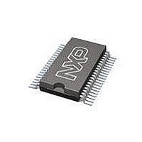
PCF8566TS/1,118 NXP Semiconductors, PCF8566TS/1,118 Datasheet - Page 7

PCF8566TS/1,118
Manufacturer Part Number
PCF8566TS/1,118
Description
IC LCD DISPLAY DVR 24SEG SOT158
Manufacturer
NXP Semiconductors
Datasheet
1.PCF8566T1118.pdf
(48 pages)
Specifications of PCF8566TS/1,118
Package / Case
40-BSOP (0.300", 7.50mm Width)
Display Type
LCD
Configuration
7 Segment + DP, 14 Segment (24 Segment)
Interface
I²C
Current - Supply
30µA
Voltage - Supply
2.5 V ~ 6 V
Operating Temperature
-40°C ~ 85°C
Mounting Type
Surface Mount
Number Of Digits
12
Number Of Segments
24
Maximum Clock Frequency
315 KHz
Operating Supply Voltage
2.5 V to 6 V
Maximum Power Dissipation
400 mW
Attached Touch Screen
No
Maximum Supply Current
90 uA
Lead Free Status / RoHS Status
Lead free / RoHS Compliant
Digits Or Characters
-
Lead Free Status / Rohs Status
Details
NXP Semiconductors
PCF8566_7
Product data sheet
7.1 Power-on reset
7.2 LCD bias generator
7.3 LCD voltage selector
At power-on the PCF8566 resets to the following starting conditions:
Do not transfer data on the I
action to complete.
The full-scale LCD voltage (V
temperature compensated externally through the V
Fractional LCD biasing voltages are obtained from an internal voltage divider comprising
three series resistors connected between V
switched out of the circuit to provide a
configuration.
The LCD voltage selector coordinates the multiplexing of the LCD in accordance with the
selected LCD drive configuration. The operation of the voltage selector is controlled by
mode-set commands from the command decoder. The biasing configurations that apply to
the preferred modes of operation, together with the biasing characteristics as functions of
V
Fig 4. Typical system configuration
•
•
•
•
•
•
•
LCD
All backplane outputs are set to V
All segment outputs are set to V
Drive mode 1:4 multiplex with
Blinking is switched off
Input and output bank selectors are reset (as defined in
The I
The data pointer and the subaddress counter are cleared
and the resulting discrimination ratios (D), are given in
V
V
DD
SS
2
C-bus interface is initialized
CONTROLLER
PROCESSOR/
MICRO-
MICRO-
HOST
R
2 C
Rev. 07 — 25 February 2009
t
rise
bus
2
C-bus after a power-on for at least 1 ms to allow the reset
oper
) is obtained from V
OSC
SDA
1
SCL
3
DD
bias is selected
DD
1
2
6
1
7
2
A0
5
bias voltage level for the 1:2 multiplex
Universal LCD driver for low multiplex rates
V
8
DD
DD
PCF8566
A1
and V
9
A2
12
V
10
17 to 40
13 to 16
LCD
LCD
SA0
DD
LCD
11
supply to pin 12.
V
. The center resistor can be
SS
V
24 segment drives
LCD
4 backplanes
Table
Table
. The LCD voltage may be
8)
5.
PCF8566
© NXP B.V. 2009. All rights reserved.
LCD PANEL
(up to 96
elements)
mgg385
7 of 48


