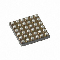
AS1119-BWLT austriamicrosystems, AS1119-BWLT Datasheet - Page 11

AS1119-BWLT
Manufacturer Part Number
AS1119-BWLT
Description
IC LED 144CH DRIVER 36WLCSP
Manufacturer
austriamicrosystems
Datasheet
1.AS1119-BWLT.pdf
(31 pages)
Specifications of AS1119-BWLT
Display Type
LED
Configuration
Dot Matrix
Interface
I²C
Current - Supply
4mA
Voltage - Supply
2.7 V ~ 5.5 V
Operating Temperature
-40°C ~ 85°C
Mounting Type
Surface Mount
Package / Case
36-UFBGA, 36-WLCSP
Lead Free Status / RoHS Status
Lead free / RoHS Compliant
Digits Or Characters
-
Other names
AS1119-BWLTTR
Available stocks
Company
Part Number
Manufacturer
Quantity
Price
Company:
Part Number:
AS1119-BWLT
Manufacturer:
MITSUBISHI
Quantity:
76
Part Number:
AS1119-BWLT
Manufacturer:
AMS
Quantity:
20 000
AS1119
Datasheet - D e t a i l e d D e s c r i p t i o n
The AS1119 can operate in the following slave modes:
I²C Device Address Byte
The address byte
Figure 16. I²C Device Address Byte
Following the START condition, the AS1119 monitors the I²C bus, checking the device type identifier being transmitted.
Upon receiving the address code, and the R/W bit, the slave device outputs an acknowledge signal on the SDA line.
www.austriamicrosystems.com/LED-Driver-ICs/AS1119
-
- Master Transmitter to Slave Receiver. The first byte transmitted by the master is the slave address, followed by
- Slave Transmitter to Master Receiver. The first byte, the slave address, is transmitted by the master. The slave
- Slave Receiver Mode. Serial data and clock are received through SDA and SCL. After each byte is received, an
- Slave Transmitter Mode. The first byte (the slave address) is received and handled as in the slave receiver
- The bit 1 and bit 2 of the address byte are the device select pins AD0 and AD1, which must be set to V
- The last bit of the address byte (R/W) define the operation to be performed. When set to a 1 a read operation is
acknowledge bit on the last byte that has been clocked out of the slave. In this case, the slave must leave the
data line HIGH to enable the master to generate the STOP condition.
Figure 15 on page 10
R/W bit, two types of data transfer are possible:
a number of data bytes. The slave returns an acknowledge bit after the slave address and each received byte.
then returns an acknowledge bit. Next, a number of data bytes are transmitted by the slave to the master. The
master returns an acknowledge bit after all received bytes other than the last byte. At the end of the last received
byte, a not-acknowledge is returned. The master device generates all of the serial clock pulses and the START
and STOP conditions. A transfer is ended with a STOP condition or a repeated START condition. Since a
repeated START condition is also the beginning of the next serial transfer, the bus will not be released.
acknowledge bit is transmitted. START and STOP conditions are recognized as the beginning and end of a serial
transfer. Address recognition is performed by hardware after reception of the slave address and direction bit.
mode. However, in this mode the direction bit will indicate that the transfer direction is reversed. Serial data is
transmitted on SDA by the AS1119 while the serial clock is input on SCL. START and STOP conditions are recog-
nized as the beginning and end of a serial transfer.
GND. A maximum of four devices with the same pre-set code can therefore be connected on the same bus at
one time.
selected; when set to a 0 a write operation is selected.
address:
(see Figure 16)
details how data transfer is accomplished on the I²C bus. Depending upon the state of the
MSB
0
is the first byte received following the START condition from the master device.
6
1
5
1
4
1
Revision 1.03
3
0
AD1
2
AD0
1
LSB
R/W
DD
or to
11 - 31


