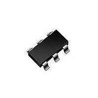
NCP1251ASN65T1G ON Semiconductor, NCP1251ASN65T1G Datasheet

NCP1251ASN65T1G
Specifications of NCP1251ASN65T1G
Available stocks
Related parts for NCP1251ASN65T1G
NCP1251ASN65T1G Summary of contents
Page 1
NCP1251 Current-Mode PWM Controller for Off-line Power Supplies The NCP1251 is a highly integrated PWM controller capable of delivering a rugged and high performance offline power supply in a tiny TSOP−6 package. With a supply range ...
Page 2
... OPTIONS Controller NCP1251ASN65T1G NCP1251BSN65T1G NCP1251ASN100T1G NCP1251BSN100T1G ORDERING INFORMATION Device Package Marking NCP1251ASN65T1G 5AA NCP1251BSN65T1G 5A2 NCP1251ASN100T1G 5AC NCP1251BSN100T1G 5AD †For information on tape and reel specifications, including part orientation and tape sizes, please refer to our Tape and Reel Packaging Specifications Brochure, BRD8011/D. ...
Page 3
OP P Vlatch Up OVP RST gone? 4 VDD R Frequency modulation Frequency foldback Vfold Vskip vdd RFB / 4 LEB Figure 2. Internal Circuit Architecture IpFlag UVLO Vcc and logic management 600 ns time constant vd d ...
Page 4
MAXIMUM RATINGS TABLE Symbol V Power Supply voltage Maximum voltage on low power pins CS, FB and OPP IOPP Maximum injected negative current into the OPP pin (pin 1) R Thermal Resistance Junction−to−Air qJA T Maximum Junction ...
Page 5
ELECTRICAL CHARACTERISTICS (For typical values T = 25°C, for min/max values T J Symbol CURRENT COMPARATOR V Default internal voltage set point for frequency foldback trip point – 45 fold V Internal peak current setpoint freeze ([31% of ...
Page 6
TEMPERATURE (°C) Figure −50 − TEMPERATURE (°C) Figure 5. ...
Page 7
TEMPERATURE (°C) Figure 9. 19.9 19.4 18.9 18.4 17.9 17.4 16.9 16.4 15.9 −50 − TEMPERATURE (°C) Figure 11 ...
Page 8
kHz SW 1.5 1 0.5 0 −50 − TEMPERATURE (°C) Figure 15 −50 − TEMPERATURE (°C) Figure 17. 390 340 290 240 ...
Page 9
TEMPERATURE (°C) Figure 21. 100 −50 − TEMPERATURE (°C) Figure 23 ...
Page 10
TEMPERATURE (°C) Figure 27. 12.9 12.4 11.9 11.4 10.9 10.4 9.9 9.4 8.9 −50 − TEMPERATURE (°C) Figure 29. 1.9 1.8 1.7 1.6 1.5 1.4 1.3 ...
Page 11
TEMPERATURE (°C) Figure 33. 390 340 290 240 190 −50 − TEMPERATURE (°C) Figure 35. 160 150 140 130 120 110 100 90 ...
Page 12
TYPICAL CHARACTERISTICS 26.9 26.4 25.9 25.4 24.9 24.4 23.9 −50 − TEMPERATURE (°C) Figure 39. http://onsemi.com 12 75 100 125 ...
Page 13
Introduction The NCP1251 implements a standard current mode architecture where the switch−off event is dictated by the peak current setpoint. This component represents the ideal candidate where low part−count and cost effectiveness are the key parameters, particularly in low−cost ac−dc ...
Page 14
D2 1N4007 12 input mains D4 1N4007 Figure 40. The Startup Resistor Can Be Connected to the Input Mains for Further Power Dissipation Reduction The first step starts with the calculation of the V capacitor which will supply the controller ...
Page 15
Internal Over Power Protection There are several known ways to implement Over Power Protection (OPP), all suffering from particular problems. These problems range from the added consumption burden on the converter or the skip−cycle disturbance brought by the current−sense offset. ...
Page 16
Let us assume that we have the following converter characteristics out 265 V in rms 1:0. 1:0. ...
Page 17
Frequency kHz min min 26 kHz 350 mV V Figure 44. By Observing the Voltage on the Feedback Pin, the Controller Reduces its Switching Frequency for an Auto−Recovery Short−Circuit Protection In case of output short−circuit or ...
Page 18
Figure 46. Inserting a Resistor in Series with the Current Sense Information Brings Ramp Compensation and In the NCP1251 controller, the oscillator ramp features a 2.5 V swing. If the clock operates kHz frequency, then ...
Page 19
ROPPL 1k C1 100p Vlatch Figure 47. A Simple Resistive Divider Brings the OPP Pin Above Case First, calculate the OPP network with the above equations. Then, suppose we want to ...
Page 20
This spike is energetic enough to charge the added capacitor C and given the time constant, 1 could make it discharge slower, potentially disturbing the blanking circuit. When implementing the Zener option important ...
Page 21
D3 15V ROPPU 841k OPP 10 4 ROPPL 2.5k 5 Vlatch Figure 50. With the NTC Back in Place, the Circuit Nicely Combines OVP, OTP and OPP on the Same Pin In nominal V / output conditions, ...
Page 22
... A 0.05 A1 *For additional information on our Pb−Free strategy and soldering details, please download the ON Semiconductor Soldering and Mounting Techniques Reference Manual, SOLDERRM/D. ON Semiconductor and are registered trademarks of Semiconductor Components Industries, LLC (SCILLC). SCILLC reserves the right to make changes without further notice to any products herein. SCILLC makes no warranty, representation or guarantee regarding the suitability of its products for any particular purpose, nor does SCILLC assume any liability arising out of the application or use of any product or circuit, and specifically disclaims any and all liability, including without limitation special, consequential or incidental damages. “ ...


