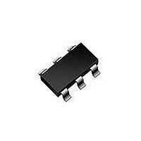
NCP1250ASN65T1G ON Semiconductor, NCP1250ASN65T1G Datasheet - Page 16

NCP1250ASN65T1G
Manufacturer Part Number
NCP1250ASN65T1G
Description
IC PWM CTLR OCP LATCH 6-TSOP
Manufacturer
ON Semiconductor
Datasheet
1.NCP1250ASN65T1G.pdf
(21 pages)
Specifications of NCP1250ASN65T1G
Output Isolation
Isolated
Frequency Range
61kHz ~ 71kHz
Voltage - Input
9.4 V ~ 28 V
Voltage - Output
12V
Operating Temperature
-40°C ~ 125°C
Package / Case
6-TSOP (0.063", 1.60mm Width)
Number Of Outputs
1
Duty Cycle (max)
84 %
Output Current
300 mA
Mounting Style
SMD/SMT
Switching Frequency
65 KHz
Operating Supply Voltage
28 V
Supply Current
2.1 mA
Maximum Operating Temperature
+ 125 C
Fall Time
30 ns
Minimum Operating Temperature
- 40 C
Rise Time
40 ns
Lead Free Status / RoHS Status
Lead free / RoHS Compliant
Available stocks
Company
Part Number
Manufacturer
Quantity
Price
Company:
Part Number:
NCP1250ASN65T1G
Manufacturer:
ON Semiconductor
Quantity:
1 250
Part Number:
NCP1250ASN65T1G
Manufacturer:
ON/安森美
Quantity:
20 000
Auto−Recovery Short−Circuit Protection
experiences a severe overloading situation, an internal error
flag is raised and starts a countdown timer. If the flag is
asserted longer than 100 ms, the driving pulses are stopped
and the V
point, the controller wakes−up and the V
Slope Compensation
signal. This is the buffered oscillator clock delivered only
during the on time. Its amplitude is around 2.5 V at the
maximum duty−cycle. Ramp compensation is a known
means used to cure sub harmonic oscillations in Continuous
Conduction
Figure 43. By Observing the Voltage on the Feedback Pin, the Controller Reduces its Switching Frequency for an
In case of output short−circuit or if the power supply
The NCP1250 includes an internal ramp compensation
FB
CC
pin slowly goes down to around 7 V. At this
Mode
Figure 44. An Auto−Recovery Hiccup Mode is Activated for Faults Longer than 100 ms
(CCM)
Frequency
65 kHz
26 kHz
−2.72
−2.72
−11.5
−11.5
23.6
23.6
14.8
14.8
6.05
6.05
F
operated
sw
−2.12
−2.12
−8.13
−8.13
min
min
15.9
15.9
9.90
9.90
3.89
3.89
V
350 mV
fold,end
445m
445m
4.32
4.32
3.35
3.35
2.38
2.38
1.41
1.41
CC
1
1
Improved Performance at Light Load
vcc
vcc
builds up again
1.5 V
V
500u
500u
current−mode
2
2
fold
vdrv
vdrv
3
3
ilprim
ilprim
http://onsemi.com
max
1.50m
1.50m
3.4 V
16
V
V
FB
FB
time in seconds
time in seconds
due to the resistive starting network. When V
VCC
absence of the fault. If the fault is still there, the supply enters
another cycle of so−called hiccup mode. If the fault has
cleared, the power supply resumes normal operation. Please
note that the soft−start is activated during each of the re−start
sequence.
converters. These oscillations take place at half the
switching frequency and occur only during CCM with a
duty−cycle greater than 50%. To lower the current loop gain,
one usually injects between 50% and 100% of the inductor
downslope. Figure 45 depicts how internally the ramp is
generated. Please note that the ramp signal will be
disconnected from the CS pin, during the off time.
2.50m
2.50m
SS
SS
ON
, the controller attempts to re−start, checking for the
Peak current setpoint
3.50m
3.50m
[
[ 0.25 V
V
V
0.36 V
V (t)
V
0.8 V
DRV
DRV
cc
cc
I
I
L
L
p
p
V
(t)
(t)
CS
4.50m
4.50m
min
V
1.05 V
freeze
1
1
2
2
3
3
V
1.5 V
fold
3.4 V
max
V
CC
FB
reaches


