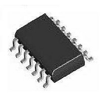
TEA1762T/N2/DG,118 NXP Semiconductors, TEA1762T/N2/DG,118 Datasheet - Page 4

TEA1762T/N2/DG,118
Manufacturer Part Number
TEA1762T/N2/DG,118
Description
IC CTLR SMPS SW SO16
Manufacturer
NXP Semiconductors
Specifications of TEA1762T/N2/DG,118
Output Voltage
3.5 V
Output Current
5 mA
Output Power
0.65 W
Duty Cycle (max)
10 %
Input Voltage
8.6 V to 38 V
Mounting Style
SMD/SMT
Package / Case
SO-14
Lead Free Status / RoHS Status
Lead free / RoHS Compliant
Other names
568-5348-2
Available stocks
Company
Part Number
Manufacturer
Quantity
Price
Part Number:
TEA1762T/N2/DG,118
Manufacturer:
NXP/恩智浦
Quantity:
20 000
NXP Semiconductors
TEA1762T_2
Product data sheet
7.1 Start-up and undervoltage lock-out
7.2 Synchronous rectification
The IC leaves the under-voltage lock-out state and activates the synchronous rectifier
circuitry and also the voltage/current sense circuitry as soon as the voltage on the V
is above 8.6 V (typical). As soon as the voltage drops below 8.1 V (typical), the
under-voltage lock-out state is re-entered and the SR driver output is actively kept low and
also the opto driver outputs are disabled.
After a negative voltage ( 310 mV typical) is sensed on the SRSENSE pin, the driver
output voltage is made high and the external MOSFET is switched on. As soon as the
SRSENSE voltage rises to 55 mV, the driver output voltage is regulated to maintain the
driver output is pulled to ground. After switch-on of the SR MOSFET, the input signal on
the SRSENSE pin is blanked for 2 s (typical). This will eliminate false switch-off due to
high frequency ringing at the start of the secondary stroke.
Because the driver output voltage is reduced as soon as the voltage on the SRSENSE pin
is 55 mV, the external power switch can be switched off fast when the current through the
switch reaches zero. With this zero-current switch off, no separate standby mode is
needed to maintain high efficiency during no-load operation. The zero current is detected
by sensing a 12 mV level on the SRSENSE pin. See
If the secondary stroke of the flyback converter is shorter than 2 s (typical), the driver
output is disabled. This will guarantee stable operation for very low duty cycles. When the
secondary stroke increases above 2.2 s (typical), the driver output is again enabled.
55 mV on the SRSENSE pin. As soon as the SRSENSE voltage is above 12 mV, the
Fig 3. Synchronous rectification
Secondary
V
SRSENSE
V
Primary
DRIVER
current
current
Rev. 02 — 25 April 2007
GreenChip synchronous rectifier controller
Figure
3.
TEA1762T
© NXP B.V. 2007. All rights reserved.
014aaa057
0 V
0 A
0 A
0 V
12 mV
55 mV
310 mV
CC
4 of 15
pin


