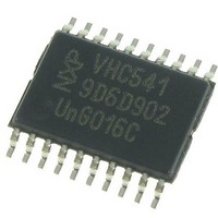
74VHC541PW,118 NXP Semiconductors, 74VHC541PW,118 Datasheet - Page 3

74VHC541PW,118
Manufacturer Part Number
74VHC541PW,118
Description
IC BUFFER/LINE DVR OCT 20TSSOP
Manufacturer
NXP Semiconductors
Series
74VHCr
Datasheet
1.74VHC541PW118.pdf
(16 pages)
Specifications of 74VHC541PW,118
Logic Type
Buffer/Line Driver, Non-Inverting
Number Of Elements
1
Number Of Bits Per Element
8
Current - Output High, Low
25mA, 25mA
Voltage - Supply
2 V ~ 5.5 V
Operating Temperature
-40°C ~ 125°C
Mounting Type
Surface Mount
Package / Case
20-TSSOP (0.173", 4.40mm Width)
Number Of Channels Per Chip
8
Polarity
Non-Inverting
Supply Voltage (max)
5.5 V
Supply Voltage (min)
2 V
Maximum Operating Temperature
+ 125 C
Mounting Style
SMD/SMT
Lead Free Status / RoHS Status
Lead free / RoHS Compliant
Other names
568-5174-2
NXP Semiconductors
5. Pinning information
Table 2.
74VHC_VHCT541_1
Product data sheet
Symbol
OE0
A[0:7]
GND
Y[0:7]
OE1
V
Fig 3.
CC
Pin configuration SO20, TSSOP20
Pin description
GND
OE0
Pin
1
2, 3, 4, 5, 6, 7, 8, 9
10
18, 17, 16, 15, 14, 13, 12, 11 data output
19
20
A0
A1
A2
A3
A4
A5
A6
A7
10
1
2
3
4
5
6
7
8
9
5.1 Pinning
5.2 Pin description
74VHCT541
74VHC541
001aak046
20
19
18
17
16
15
14
13
12
11
Description
output enable input (active LOW)
data input
ground (0 V)
output enable input (active LOW)
supply voltage
V
OE1
Y0
Y1
Y2
Y3
Y4
Y5
Y6
Y7
CC
Rev. 01 — 12 August 2009
Fig 4.
(1) The die substrate is attached to this pad using
74VHC541; 74VHCT541
conductive die attach material. It can not be used as a
supply pin or input.
Pin configuration DHVQFN20
index area
terminal 1
A0
A1
A2
A3
A4
A5
A6
A7
Transparent top view
2
3
4
5
6
7
8
9
Octal buffer/line driver; 3-state
74VHCT541
74VHC541
GND
(1)
19
18
17
16
15
14
13
12
001aak047
© NXP B.V. 2009. All rights reserved.
OE1
Y0
Y1
Y2
Y3
Y4
Y5
Y6
3 of 16


