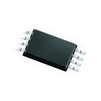
NX3V1T66GW,125 NXP Semiconductors, NX3V1T66GW,125 Datasheet - Page 2

NX3V1T66GW,125
Manufacturer Part Number
NX3V1T66GW,125
Description
IC ANALOG SWITCH SPST UMT5
Manufacturer
NXP Semiconductors
Datasheet
1.NX3V1T66GM132.pdf
(20 pages)
Specifications of NX3V1T66GW,125
Number Of Switches
1
Switch Configuration
SPST
On Resistance (max)
0.8 Ohms
On Time (max)
57 ns
Off Time (max)
90 ns
Off Isolation (typ)
- 90 dB
Supply Voltage (max)
4.3 V
Supply Voltage (min)
1.4 V
Supply Current
690 nA, 800 nA
Maximum Power Dissipation
250 mW
Maximum Operating Temperature
+ 125 C
Mounting Style
SMD/SMT
Package / Case
TSSOP-5
Minimum Operating Temperature
- 40 C
Off State Leakage Current (max)
+/- 500 nA
Operating Frequency
25 MHz
Power Dissipation
250 mW
Switch Current (typ)
+/- 500 mA, +/- 750 mA
Lead Free Status / RoHS Status
Lead free / RoHS Compliant
Other names
568-5568-2
NXP Semiconductors
3. Applications
4. Ordering information
Table 1.
5. Marking
Table 2.
[1]
6. Functional diagram
NX3V1T66
Product data sheet
Type number
NX3V1T66GW
NX3V1T66GM
Type number
NX3V1T66GW
NX3V1T66GM
Fig 1.
The pin 1 indicator is located on the lower left corner of the device, below the marking code.
Logic symbol
Ordering information
Marking codes
Package
Temperature range Name
40 C to +125 C
40 C to +125 C
E
Z
[1]
Cell phone
PDA
Portable media player
001aag487
Y
All information provided in this document is subject to legal disclaimers.
TSSOP5 plastic thin shrink small outline package; 5 leads;
XSON6
Rev. 6 — 21 December 2010
Description
body width 1.25 mm
plastic extremely thin small outline package; no leads;
6 terminals; body 1 1.45 0.5 mm
Marking code
dO
dO
Fig 2.
Low-ohmic single-pole single-throw analog switch
Logic diagram
Y
E
NX3V1T66
001aah372
© NXP B.V. 2010. All rights reserved.
Z
Version
SOT353-1
SOT886
2 of 20


