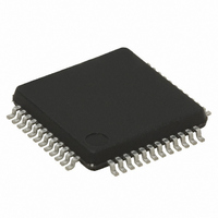
STM8S207C8T3 STMicroelectronics, STM8S207C8T3 Datasheet - Page 32

STM8S207C8T3
Manufacturer Part Number
STM8S207C8T3
Description
IC MCU 8BIT 64KB FLASH 48LQFP
Manufacturer
STMicroelectronics
Series
STM8Sr
Datasheet
1.STEVAL-MKI030V1.pdf
(105 pages)
Specifications of STM8S207C8T3
Featured Product
STM32 Cortex-M3 Companion Products
Core Processor
STM8
Core Size
8-Bit
Speed
24MHz
Connectivity
I²C, IrDA, LIN, SPI, UART/USART
Peripherals
Brown-out Detect/Reset, POR, PWM, WDT
Number Of I /o
38
Program Memory Size
64KB (64K x 8)
Program Memory Type
FLASH
Eeprom Size
1.5K x 8
Ram Size
4K x 8
Voltage - Supply (vcc/vdd)
2.95 V ~ 5.5 V
Data Converters
A/D 10x10b
Oscillator Type
Internal
Operating Temperature
-40°C ~ 125°C
Package / Case
48-LFQFP
Core
STM8
Lead Free Status / RoHS Status
Lead free / RoHS Compliant
Available stocks
Company
Part Number
Manufacturer
Quantity
Price
Company:
Part Number:
STM8S207C8T3
Manufacturer:
ST
Quantity:
1 000
Company:
Part Number:
STM8S207C8T3
Manufacturer:
STMicroelectronics
Quantity:
10 000
Pinouts and pin description
Table 6.
1. The default state of UART1_RX and UART3_RX pins is controlled by the ROM bootloader. These pins are pulled up as
2. The beCAN interface is available on STM8S208xx devices only
3. In the open-drain output column, ‘T’ defines a true open-drain I/O (P-buffer, weak pull-up, and protection diode to V
4. The PD1 pin is in input pull-up during the reset phase and after the internal reset release.
5. Available in 44-pin package only. On other packages, the AFR4 bit is reserved and must be kept at 0.
32/105
65 51
66 52
67 53 37
68 54 38 34
69 55 39 35
70 56 40 36
71
72
73 57 41 37 25 PD0/TIM3_CH2
74 58 42 38 26 PD1/SWIM
75 59 43 39 27 PD2/TIM3_CH1
76 60 44 40 28 PD3/TIM2_CH2
77 61 45 41 29
78 62 46 42 30 PD5/ UART3_TX
79 63 47 43 31
80 64 48 44 32 PD7/TLI
part of the bootloader activation process and returned to the floating state before a return from the bootloader.
not implemented).
Pin number
-
-
-
-
-
-
Pin description (continued)
-
-
-
-
-
- PG7
- PE4
- PE3/TIM1_BKIN
- PE2/I
- PE1/I
- PE0/CLK_CCO
- PI6
- PI7
PD4/TIM2_CH1/B
EEP
PD6/
UART3_RX
Pin name
2
2
C_SDA
C_SCL
(4)
(1)
I/O X
I/O X
I/O X
I/O X
I/O X
I/O X
I/O X
I/O X
I/O X
I/O X
I/O X
I/O X
I/O X
I/O X
I/O X
I/O X
Doc ID 14733 Rev 11
Input
X
X
X
X
X
X
X
X
X
X
X
X
X
X
X
X
X
X
X HS O3 X
X HS O3 X
X HS O4 X
X HS O3 X
X HS O3 X
X HS O3 X
X
X
X
Output
O1 X
O1 X
O1 X
O1 T
O1 T
O1 X
O1 X
O1 X
O1 X
O1 X
(3)
(3)
X Port G7
X Port E4
X Port E3
X Port E0
X
X
X Port D0
X Port D1
X Port D2
X Port D3
X Port D4
X Port D5
X Port D6
X Port D7
Port E2 I
Port E1 I
Port I6
Port I7
STM8S207xx, STM8S208xx
Timer 1 -
break input
Configurable
clock output
Timer 3 -
channel 2
SWIM data
interface
Timer 3 -
channel 1
Timer 2 -
channel 2
Timer 2 -
channel 1
UART3 data
transmit
UART3 data
receive
Top level
interrupt
2
2
C data
C clock
alternate
function
Default
TIM1_BKIN
[AFR3]/
CLK_CCO
[AFR2]
TIM2_CH3
[AFR1]
ADC_ETR
[AFR0]
BEEP output
[AFR7]
TIM1_CH4
[AFR4]
after remap
[option bit]
Alternate
function
DD
are
(5)


