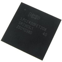
LPC2420FET208,551 NXP Semiconductors, LPC2420FET208,551 Datasheet - Page 10

LPC2420FET208,551
Manufacturer Part Number
LPC2420FET208,551
Description
IC ARM7 MCU 16BIT T208FBGA
Manufacturer
NXP Semiconductors
Series
LPC2400r
Datasheet
1.LPC2460FBD208551.pdf
(79 pages)
Specifications of LPC2420FET208,551
Core Processor
ARM7
Core Size
16/32-Bit
Speed
72MHz
Connectivity
EBI/EMI, I²C, Microwire, MMC, SPI, SSI, SSP, UART/USART, USB OTG
Peripherals
Brown-out Detect/Reset, DMA, I²S, POR, PWM, WDT
Number Of I /o
160
Program Memory Type
ROMless
Ram Size
82K x 8
Voltage - Supply (vcc/vdd)
3 V ~ 3.6 V
Data Converters
A/D 8x10b; D/A 1x10b
Oscillator Type
Internal
Operating Temperature
-40°C ~ 85°C
Package / Case
208-TFBGA
Processor Series
LPC2420
Core
ARM7
Data Bus Width
16 bit, 32 bit
Data Ram Size
98 KB
Interface Type
SPI, I2C, I2S, USB, SSP
Maximum Clock Frequency
72 MHz
Number Of Programmable I/os
160
Number Of Timers
4
Maximum Operating Temperature
+ 85 C
Mounting Style
SMD/SMT
Minimum Operating Temperature
- 40 C
Processor To Be Evaluated
ARM7TDMI-S
Lead Free Status / RoHS Status
Lead free / RoHS Compliant
Program Memory Size
-
Eeprom Size
-
Lead Free Status / Rohs Status
Details
Other names
568-5216
Available stocks
Company
Part Number
Manufacturer
Quantity
Price
Company:
Part Number:
LPC2420FET208,551
Manufacturer:
MAX
Quantity:
65
Company:
Part Number:
LPC2420FET208,551
Manufacturer:
NXP Semiconductors
Quantity:
10 000
NXP Semiconductors
Table 4.
LPC2420_60_5
Preliminary data sheet
Symbol
P0[3]/RXD0
P0[4]/
I2SRX_CLK/
RD2/CAP2[0]
P0[5]/
I2SRX_WS/
TD2/CAP2[1]
P0[6]/
I2SRX_SDA/
SSEL1/MAT2[0]
P0[7]/
I2STX_CLK/
SCK1/MAT2[1]
P0[8]/
I2STX_WS/
MISO1/MAT2[2]
P0[9]/
I2STX_SDA/
MOSI1/MAT2[3]
P0[10]/TXD2/
SDA2/MAT3[0]
P0[11]/RXD2/
SCL2/MAT3[1]
Pin description
Pin
204
168
166
164
162
160
158
98
100
[1]
[1]
[1]
[1]
[1]
[1]
[1]
[1]
[1]
…continued
Ball
D6
B12
C12
D13
C13
A15
C14
T15
R14
[1]
[1]
[1]
[1]
[1]
[1]
[1]
[1]
[1]
Type
I/O
I
I/O
I/O
I
I
I/O
I/O
O
I
I/O
I/O
I/O
O
I/O
I/O
I/O
O
I/O
I/O
I/O
O
I/O
I/O
I/O
O
I/O
O
I/O
O
I/O
I
I/O
O
Rev. 05 — 24 February 2010
Description
P0[3] — General purpose digital input/output pin.
RXD0 — Receiver input for UART0.
P0[4] — General purpose digital input/output pin.
I2SRX_CLK — Receive Clock. It is driven by the master and received by
the slave. Corresponds to the signal SCK in the I
RD2 — CAN2 receiver input (LPC2460 only).
CAP2[0] — Capture input for Timer 2, channel 0.
P0[5] — General purpose digital input/output pin.
I2SRX_WS — Receive Word Select. It is driven by the master and
received by the slave. Corresponds to the signal WS in the I
specification.
TD2 — CAN2 transmitter output (LPC2460 only).
CAP2[1] — Capture input for Timer 2, channel 1.
P0[6] — General purpose digital input/output pin.
I2SRX_SDA — Receive data. It is driven by the transmitter and read by
the receiver. Corresponds to the signal SD in the I
SSEL1 — Slave Select for SSP1.
MAT2[0] — Match output for Timer 2, channel 0.
P0[7] — General purpose digital input/output pin.
I2STX_CLK — Transmit Clock. It is driven by the master and received by
the slave. Corresponds to the signal SCK in the I
SCK1 — Serial Clock for SSP1.
MAT2[1] — Match output for Timer 2, channel 1.
P0[8] — General purpose digital input/output pin.
I2STX_WS — Transmit Word Select. It is driven by the master and
received by the slave. Corresponds to the signal WS in the I
specification.
MISO1 — Master In Slave Out for SSP1.
MAT2[2] — Match output for Timer 2, channel 2.
P0[9] — General purpose digital input/output pin.
I2STX_SDA — Transmit data. It is driven by the transmitter and read by
the receiver. Corresponds to the signal SD in the I
MOSI1 — Master Out Slave In for SSP1.
MAT2[3] — Match output for Timer 2, channel 3.
P0[10] — General purpose digital input/output pin.
TXD2 — Transmitter output for UART2.
SDA2 — I
MAT3[0] — Match output for Timer 3, channel 0.
P0[11] — General purpose digital input/output pin.
RXD2 — Receiver input for UART2.
SCL2 — I
MAT3[1] — Match output for Timer 3, channel 1.
2
2
C2 clock input/output (this is not an open-drain pin).
C2 data input/output (this is not an open-drain pin).
Flashless 16-bit/32-bit microcontroller
LPC2420/2460
2
2
S-bus specification.
S-bus specification.
2
2
S-bus specification.
S-bus specification.
© NXP B.V. 2010. All rights reserved.
2
2
S-bus
S-bus
10 of 79


