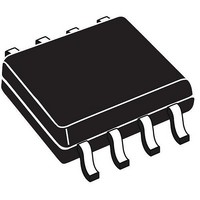
PCF8563T/5,518 NXP Semiconductors, PCF8563T/5,518 Datasheet - Page 22

PCF8563T/5,518
Manufacturer Part Number
PCF8563T/5,518
Description
IC RTC/CALENDAR 8SOIC
Manufacturer
NXP Semiconductors
Type
Clock/Calendarr
Datasheet
1.PCF8563TF4118.pdf
(45 pages)
Specifications of PCF8563T/5,518
Package / Case
*
Time Format
HH:MM:SS (24 hr)
Date Format
YY-MM-DD-dd
Memory Size
128b (16 x 8)
Interface
I²C, 2-Wire Serial
Voltage - Supply
1.8 V ~ 5.5 V
Operating Temperature
-40°C ~ 85°C
Mounting Type
*
Function
Clock, Calendar, Alarm, Timer
Supply Voltage (max)
5.5 V
Supply Voltage (min)
1 V
Maximum Operating Temperature
+ 85 C
Minimum Operating Temperature
- 40 C
Mounting Style
SMD/SMT
Rtc Bus Interface
I2C
Supply Current
+/- 50 mA
Bus Type
Serial (2-Wire, I2C)
Operating Supply Voltage (typ)
2.5/3.3/5V
Package Type
SO
Operating Supply Voltage (max)
5.5V
Operating Supply Voltage (min)
1.8V
Operating Temperature Classification
Industrial
Operating Temperature (max)
85C
Operating Temperature (min)
-40C
Pin Count
8
Mounting
Surface Mount
Lead Free Status / RoHS Status
Lead free / RoHS Compliant
Lead Free Status / RoHS Status
Lead free / RoHS Compliant, Lead free / RoHS Compliant
Other names
568-6650-2
PCF8563T/5,518
PCF8563T/5,518
NXP Semiconductors
PCF8563
Product data sheet
Fig 16. System configuration
SDA
SCL
TRANSMITTER
9.4 Acknowledge
RECEIVER
MASTER
The number of data bytes transferred between the START and STOP conditions from
transmitter to receiver is unlimited. Each byte of eight bits is followed by an acknowledge
cycle.
Acknowledgement on the I
Fig 17. Acknowledgement on the I
•
•
•
•
A slave receiver, which is addressed, must generate an acknowledge after the
reception of each byte.
Also a master receiver must generate an acknowledge after the reception of each
byte that has been clocked out of the slave transmitter.
The device that acknowledges must pull-down the SDA line during the acknowledge
clock pulse, so that the SDA line is stable LOW during the HIGH period of the
acknowledge related clock pulse (set-up and hold times must be taken into
consideration).
A master receiver must signal an end of data to the transmitter by not generating an
acknowledge on the last byte that has been clocked out of the slave. In this event, the
transmitter must leave the data line HIGH to enable the master to generate a STOP
condition.
by transmitter
data output
by receiver
data output
SCL from
master
RECEIVER
SLAVE
All information provided in this document is subject to legal disclaimers.
condition
START
Rev. 8 — 18 November 2010
S
2
C-bus is illustrated in
TRANSMITTER
RECEIVER
SLAVE
1
2
C-bus
2
TRANSMITTER
Figure
MASTER
17.
not acknowledge
acknowledge
Real-time clock/calendar
8
TRANSMITTER
RECEIVER
MASTER
acknowledgement
clock pulse for
PCF8563
© NXP B.V. 2010. All rights reserved.
mba605
9
mbc602
22 of 45


