IP4305CX4/LF/P,315 NXP Semiconductors, IP4305CX4/LF/P,315 Datasheet
IP4305CX4/LF/P,315
Specifications of IP4305CX4/LF/P,315


Related parts for IP4305CX4/LF/P,315


IP4305CX4/LF/P,315 Summary of contents
Page 1
IP4305CX4/LF (/P) Integrated dual Schottky diode array with ESD protection to IEC61000-4-2, level 4 20 August 2009 1. Product profile 1.1 General description IP4305CX4/LF (/ dual Schottky diode – one back-2-back diode array ...
Page 2
... NXP Semiconductors 3. Limiting values Table 1. Symbol Parameter V DC input voltage range for A1 to A2 input voltage range for I/O ESD Electrostatic Discharge Pins (B2, A2 connected to an 2kV compliant IC I/O) Pins to B2 with B1 unconnected P Maximum continuous power dissipation D-ch per channel T storage temperature range ...
Page 3
... NXP Semiconductors 5. Design/Assembly Recommendations 5.1 PCB Design Guidelines For the optimum performance, a Non-Solder Mask PCB design (NSMD), also known as a copper- defined design, incorporating laser-drilled micro-vias connecting the ground pads to a buried ground-plane layer is recommended. This results in the lowest possible ground inductance and provides the best high frequency and ESD performance ...
Page 4
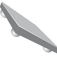
... NXP Semiconductors 6. Package outline Fig 4. IP4305CX4/LF (/P) outline dimensions Product data sheet IP4305CX4/LF (/P) Integrated dual Schottky diode array with ESD protection 0.61 ±0.04 ±0.05 B1 0.26 B2 ±0.05 0.41 ±0.05 ±0.02 Side view Bottom view, balls facing up Pin A1 index area A1 B1 Laser marking area ...
Page 5
... NXP Semiconductors 7. Tape & Reel information OVERALL DIMENSIONS SPROCKET HOLES DISTANCE BETWEEN CENTRE LINES COMPARTMENTS DEVICE CARRIER TAPE ANTISTATIC COVER TAPE BENDING RAD Fig 5. IP4305CX4/LF (/P) Tape & Reel information Product data sheet IP4305CX4/LF (/P) Integrated dual Schottky diode array with ESD protection ...
Page 6
... NXP Semiconductors. In case of any inconsistency or conflict between information in this document and such terms and conditions, the latter will prevail. ...
Page 7
... NXP Semiconductors 10. Contents 1. Product profile.....................................................1 1.1 General description ............................................1 1.2 Features .............................................................1 1.3 Applications........................................................1 2. Pinning Information ............................................1 3. Limiting values ....................................................2 4. Electrical Characteristics ...................................2 5. Design/Assembly Recommendations ...............3 5.1 PCB Design Guidelines......................................3 5.2 PCB Assembly Guidelines for Pb-free soldering 3 6. Package outline ...................................................4 7. Tape & Reel information .....................................5 8 ...