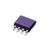
DG419DY-T1-E3 Vishay, DG419DY-T1-E3 Datasheet - Page 14

DG419DY-T1-E3
Manufacturer Part Number
DG419DY-T1-E3
Description
Analog Switch ICs Single SPDT 22/25V
Manufacturer
Vishay
Type
Analog Switchr
Specifications of DG419DY-T1-E3
Number Of Switches
Single
Switch Configuration
SPDT
On Resistance (max)
40 Ohms (Typ) @ 10.8 V
On Time (max)
110 ns (Typ) @ 12 V
Off Time (max)
40 ns (Typ) @ 12 V
Supply Voltage (max)
25 V
Supply Current
0.000001 mA
Maximum Power Dissipation
400 mW
Maximum Operating Temperature
+ 85 C
Mounting Style
SMD/SMT
Package / Case
SOIC-8 Narrow
Minimum Operating Temperature
- 40 C
Propagation Delay Time
175 ns
Analog Switch Type
SPDT
No. Of Channels
1
On State Resistance Max
20ohm
Turn Off Time
40ns
Turn On Time
110ns
Supply Voltage Range
± 15V
Operating Temperature Range
-40°C To +85°C
Multiplexer Configuration
Single SPDT
Number Of Inputs
1
Number Of Outputs
2
Number Of Channels
1
Analog Switch On Resistance
45@±13.5VOhm
Package Type
SOIC N
Power Supply Requirement
Single/Dual
Single Supply Voltage (min)
13V
Single Supply Voltage (typ)
15/18/24/28V
Single Supply Voltage (max)
36V
Dual Supply Voltage (min)
±7V
Dual Supply Voltage (typ)
±9/±12/±15/±18V
Dual Supply Voltage (max)
±22V
Power Dissipation
400mW
Mounting
Surface Mount
Pin Count
8
Operating Temp Range
-40C to 85C
Operating Temperature Classification
Industrial
Lead Free Status / RoHS Status
Lead free / RoHS Compliant
Lead Free Status / RoHS Status
Lead free / RoHS Compliant, Lead free / RoHS Compliant
Available stocks
Company
Part Number
Manufacturer
Quantity
Price
Company:
Part Number:
DG419DY-T1-E3
Manufacturer:
SAMSUNG
Quantity:
2 854
Part Number:
DG419DY-T1-E3
Manufacturer:
VISHAY/威世
Quantity:
20 000
Wharton McDaniel
Surface-mounted LITTLE FOOT power MOSFETs use
integrated circuit and small-signal packages which have
been been modified to provide the heat transfer capabilities
required by power devices. Leadframe materials and
design, molding compounds, and die attach materials have
been changed, while the footprint of the packages remains
the same.
See Application Note 826, Recommended Minimum Pad
Patterns With Outline Drawing Access for Vishay Siliconix
MOSFETs, (http://www.vishay.com/ppg?72286), for the
basis of the pad design for a LITTLE FOOT SO-8 power
MOSFET. In converting this recommended minimum pad
to the pad set for a power MOSFET, designers must make
two connections: an electrical connection and a thermal
connection, to draw heat away from the package.
In the case of the SO-8 package, the thermal connections
are very simple. Pins 5, 6, 7, and 8 are the drain of the
MOSFET for a single MOSFET package and are connected
together. In a dual package, pins 5 and 6 are one drain, and
pins 7 and 8 are the other drain. For a small-signal device or
integrated circuit, typical connections would be made with
traces that are 0.020 inches wide. Since the drain pins serve
the additional function of providing the thermal connection
to the package, this level of connection is inadequate. The
total cross section of the copper may be adequate to carry
the current required for the application, but it presents a
large thermal impedance. Also, heat spreads in a circular
fashion from the heat source. In this case the drain pins are
the heat sources when looking at heat spread on the PC
board.
Document Number: 70740
Revision: 18-Jun-07
TrenchFET
Mounting LITTLE FOOT
0.050
0.027
1.27
0.69
Figure 1. Single MOSFET SO-8 Pad
Pattern With Copper Spreading
®
0.078
1.98
Power MOSFETs
V I S H A Y S I L I C O N I X
0.288
7.3
5.07
0.2
0.196
5.0
®
, SO-8 Power MOSFETs
The minimum recommended pad patterns for the
single-MOSFET SO-8 with copper spreading (Figure 1) and
dual-MOSFET SO-8 with copper spreading (Figure 2) show
the starting point for utilizing the board area available for the
heat-spreading copper. To create this pattern, a plane of
copper overlies the drain pins. The copper plane connects
the drain pins electrically, but more importantly provides
planar copper to draw heat from the drain leads and start the
process of spreading the heat so it can be dissipated into the
ambient air. These patterns use all the available area
underneath the body for this purpose.
Since surface-mounted packages are small, and reflow
soldering is the most common way in which these are
affixed to the PC board, “thermal” connections from the
planar copper to the pads have not been used. Even if
additional planar copper area is used, there should be no
problems in the soldering process. The actual solder
connections are defined by the solder mask openings. By
combining the basic footprint with the copper plane on the
drain pins, the solder mask generation occurs automatically.
A final item to keep in mind is the width of the power traces.
The absolute minimum power trace width must be
determined by the amount of current it has to carry. For
thermal reasons, this minimum width should be at least
0.020 inches. The use of wide traces connected to the drain
plane provides a low impedance path for heat to move away
from the device.
0.050
0.027
1.27
0.69
Figure 2. Dual MOSFET SO-8 Pad Pattern
0.078
1.98
With Copper Spreading
0.288
7.3
Application Note 808
5.07
0.2
www.vishay.com
0.088
0.088
2.25
2.25
1


