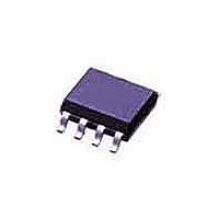
DG419LDY-E3 Vishay, DG419LDY-E3 Datasheet - Page 10

DG419LDY-E3
Manufacturer Part Number
DG419LDY-E3
Description
Analog Switch ICs SPDT Analog Switch
Manufacturer
Vishay
Type
Analog Switchr
Specifications of DG419LDY-E3
Number Of Switches
Single
Switch Configuration
SPDT
On Resistance (max)
70 Ohms
On Time (max)
75 ns
Off Time (max)
41 ns
Supply Voltage (max)
12 V
Supply Voltage (min)
2.7 V
Supply Current
0.00002 mA
Maximum Power Dissipation
400 mW
Maximum Operating Temperature
+ 85 C
Mounting Style
SMD/SMT
Package / Case
SOIC-8 Narrow
Minimum Operating Temperature
- 40 C
Propagation Delay Time
47 ns
Analog Switch Type
SPDT
No. Of Channels
1
On State Resistance Max
18.5ohm
Turn Off Time
32ns
Turn On Time
41ns
Supply Voltage Range
2.7V To 12V
Operating Temperature Range
-40°C To +85°C
Package
8SOIC N
Maximum On Resistance
70@2.7V Ohm
Maximum Propagation Delay Bus To Bus
47@±5V ns
Maximum High Level Output Current
30 mA
Maximum Turn-off Time
41@3V ns
Maximum Turn-on Time
75@3V ns
Switch Architecture
SPDT
Power Supply Type
Single|Dual
Lead Free Status / RoHS Status
Lead free / RoHS Compliant
Lead Free Status / RoHS Status
Lead free / RoHS Compliant, Lead free / RoHS Compliant
Available stocks
Company
Part Number
Manufacturer
Quantity
Price
DG417, DG418, DG419
Vishay Siliconix
APPLICATIONS
Micropower UPS Transfer Switch
When V
closing SW
Figure 10. D
rest of the circuit. Current consumption by the CMOS analog
switch is around 100 pA; this ensures that most of the power
available is applied to the memory, where it is really needed.
In the stand-by mode, hundreds of A are sufficient to retain
memory data.
When the 5 V supply comes back up, the resistor divider
senses the presence of at least 3.5 V, and causes a new
change of state in the analog switch, restoring normal
operation.
Vishay Siliconix maintains worldwide manufacturing capability. Products may be manufactured at one of several qualified locations. Reliability data for Silicon
Technology and Package Reliability represent a composite of all qualified locations. For related documents such as package/tape drawings, part marking, and
reliability data, see www.vishay.com/ppg?70051.
www.vishay.com
10
V
IN
CC
Figure 12. Programmable Gain Amplifier
1
1
drops to 3.3 V, the DG417 changes states,
and connecting the backup cell, as shown in
prevents current from leaking back towards the
IN
V
(5 V)
CC
D
DG419
-
+
R
453 k
R
383 k
1
2
S
S
1
2
D
1
V
SENSE
R
R
1
2
Figure 11. Micropower UPS Circuit
Memory
V
OUT
Programmable Gain Amplifier
The DG419, as shown in figure 11, allows accurate gain
selection in a small package. Switching into virtual ground
reduces distortion caused by R
of analog signal amplitude.
GaAs FET Driver
The DG419, as shown in figure 12 may be used as a GaAs
FET driver. It translates a TTL control signal into - 8 V, 0 V
level outputs to drive the gate.
5 V
D
GND
IN
V+
DG417
SW
1
V
V-
L
Figure 13. GaAs FET Driver
S
S
S
GND
1
2
V
L
DG419
DS(on)
+ 5 V
- 8 V
V+
V-
+
–
S10-1528-Rev. G, 19-Jul-10
Document Number: 70051
3 V Li Cell
D
variation as a function
V
OUT
GaAs FET


