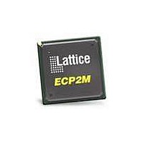
LFE2M20E-5FN256C Lattice, LFE2M20E-5FN256C Datasheet - Page 36

LFE2M20E-5FN256C
Manufacturer Part Number
LFE2M20E-5FN256C
Description
FPGA - Field Programmable Gate Array 19K LUTs 140 I/O SERDES DSP -5
Manufacturer
Lattice
Datasheet
1.LFE2-12SE-6FN256C.pdf
(389 pages)
Specifications of LFE2M20E-5FN256C
Number Of Macrocells
19000
Maximum Operating Frequency
311 MHz
Number Of Programmable I/os
140
Data Ram Size
1246208
Supply Voltage (max)
1.26 V
Maximum Operating Temperature
+ 85 C
Minimum Operating Temperature
0 C
Mounting Style
SMD/SMT
Supply Voltage (min)
1.14 V
Package / Case
FPBGA-256
Lead Free Status / RoHS Status
Lead free / RoHS Compliant
Available stocks
Company
Part Number
Manufacturer
Quantity
Price
Company:
Part Number:
LFE2M20E-5FN256C
Manufacturer:
Lattice Semiconductor Corporation
Quantity:
10 000
- Current page: 36 of 389
- Download datasheet (5Mb)
Lattice Semiconductor
Figure 2-30. Input Register Block Top Edge
Output Register Block
The output register block provides the ability to register signals from the core of the device before they are passed
to the sysI/O buffers. The blocks on the PIOs on the left, right and bottom contain a register for SDR operation that
is combined with an additional latch for DDR operation. Figure 2-31 shows the diagram of the Output Register
Block for PIOs on the left, right and the bottom edges. Figure 2-32 shows the diagram of the Output Register Block
for PIOs on the top edge of the device.
In SDR mode, ONEG0 feeds one of the flip-flops that then feeds the output. The flip-flop can be configured as a D-
type or latch. In DDR mode, ONEG0 and OPOS0 are fed into registers on the positive edge of the clock. Then at
the next clock cycle this registered OPOS0 is latched. A multiplexer running off the same clock selects the correct
register for feeding to the output (D0).
By combining the output blocks of the complementary PIOs and sharing some registers from input blocks, a gear-
box function can be implemented, that takes four data streams: ONEG0A, ONEG1A, ONEG1B and ONEG1B.
Figure 2-32 shows the diagram using this gearbox function. For more information about this topic, please see infor-
mation regarding additional documentation at the end of this data sheet.
(from sysIO
DEL[3:0]
routing)
buffer)
CLK0
(from
DI
Note: Simplified version does not show CE and SET/RESET details.
*On selected blocks.
Fixed Delay
Dynamic Delay
2-33
D
/LATCH
D-Type
LatticeECP2/M Family Data Sheet
Q
INCK*
INDD
IPOS0
Architecture
Related parts for LFE2M20E-5FN256C
Image
Part Number
Description
Manufacturer
Datasheet
Request
R

Part Number:
Description:
FPGA - Field Programmable Gate Array 19K LUTs 304 I/O SERDES DSP -5
Manufacturer:
Lattice
Datasheet:

Part Number:
Description:
FPGA - Field Programmable Gate Array 19K LUTs 304 I/O SERDES DSP -5
Manufacturer:
Lattice

Part Number:
Description:
FPGA - Field Programmable Gate Array 19K LUTs 304 I/O SERDES DSP -6
Manufacturer:
Lattice
Datasheet:

Part Number:
Description:
FPGA - Field Programmable Gate Array 19K LUTs 140 I/O SERDES DSP -6
Manufacturer:
Lattice
Datasheet:
Part Number:
Description:
FPGA LatticeECP2M Family 19000 Cells 90nm (CMOS) Technology 1.2V 484-Pin FBGA
Manufacturer:
LATTICE SEMICONDUCTOR
Datasheet:
Part Number:
Description:
FPGA LatticeECP2M Family 19000 Cells 90nm (CMOS) Technology 1.2V 256-Pin FBGA
Manufacturer:
LATTICE SEMICONDUCTOR
Datasheet:
Part Number:
Description:
FPGA LatticeECP2M Family 19000 Cells 90nm (CMOS) Technology 1.2V 256-Pin FBGA
Manufacturer:
LATTICE SEMICONDUCTOR
Datasheet:

Part Number:
Description:
IC FPGA 20KLUTS 140I/O 256-BGA
Manufacturer:
Lattice
Datasheet:

Part Number:
Description:
IC FPGA 20KLUTS 140I/O 256-BGA
Manufacturer:
Lattice
Datasheet:

Part Number:
Description:
IC FPGA 20KLUTS 140I/O 256-BGA
Manufacturer:
Lattice
Datasheet:

Part Number:
Description:
IC FPGA 20KLUTS 304I/O 484-BGA
Manufacturer:
Lattice
Datasheet:

Part Number:
Description:
IC FPGA 20KLUTS 140I/O 256-BGA
Manufacturer:
Lattice
Datasheet:

Part Number:
Description:
IC FPGA 20KLUTS 140I/O 256-BGA
Manufacturer:
Lattice
Datasheet:

Part Number:
Description:
IC FPGA 20KLUTS 304I/O 484-BGA
Manufacturer:
Lattice
Datasheet:


