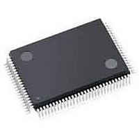
A54SX32A-TQG100 Actel, A54SX32A-TQG100 Datasheet - Page 6

A54SX32A-TQG100
Manufacturer Part Number
A54SX32A-TQG100
Description
FPGA - Field Programmable Gate Array 48K System Gates
Manufacturer
Actel
Datasheet
1.A54SX08A-TQG100.pdf
(108 pages)
Specifications of A54SX32A-TQG100
Processor Series
A54SX32
Core
IP Core
Number Of Macrocells
1800
Maximum Operating Frequency
350 MHz
Number Of Programmable I/os
249
Delay Time
4 ns to 8.4 ns
Supply Voltage (max)
5.25 V
Maximum Operating Temperature
+ 70 C
Minimum Operating Temperature
0 C
Development Tools By Supplier
Silicon-Explorer II, Silicon-Sculptor 3, SI-EX-TCA
Mounting Style
SMD/SMT
Supply Voltage (min)
2.25 V
Number Of Gates
32 K
Package / Case
TQFP-100
Lead Free Status / RoHS Status
Lead free / RoHS Compliant
Available stocks
Company
Part Number
Manufacturer
Quantity
Price
Company:
Part Number:
A54SX32A-TQG100
Manufacturer:
Microsemi SoC
Quantity:
10 000
Part Number:
A54SX32A-TQG100
Manufacturer:
MICROSEMI/美高森美
Quantity:
20 000
Company:
Part Number:
A54SX32A-TQG100A
Manufacturer:
Microsemi SoC
Quantity:
10 000
Company:
Part Number:
A54SX32A-TQG100I
Manufacturer:
Microsemi SoC
Quantity:
10 000
Logic Module Design
The SX-A family architecture is described as a “sea-of-
modules” architecture because the entire floor of the
device is covered with a grid of logic modules with
virtually no chip area lost to interconnect elements or
routing. The Actel SX-A family provides two types of
logic modules: the register cell (R-cell) and the
combinatorial cell (C-cell).
The R-cell contains a flip-flop featuring asynchronous clear,
asynchronous preset, and clock enable, using the S0 and S1
lines control signals
programmable clock polarity selectable on a register-by-
register basis. This provides additional flexibility while
allowing mapping of synthesized functions into the SX-A
FPGA. The clock source for the R-cell can be chosen from
either the hardwired clock, the routed clocks, or internal
logic.
The C-cell implements a range of combinatorial functions
of up to five inputs
and its associated inverter function allows up to 4,000
Figure 1-2 • R-Cell
Figure 1-3 • C-Cell
1 -2
SX-A Family FPGAs
(Figure
(Figure
1-2). The R-cell registers feature
1-3). Inclusion of the DB input
DirectConnect
Internal Logic
DB
D0
D1
D2
D3
CLKA,
HCLK
CLKB,
Input
CKS
S0
Data Input
Routed
A0 B0
v5.3
Sa
different combinatorial functions to be implemented in a
single module. An example of the flexibility enabled by
the inversion capability is the ability to integrate a 3-input
exclusive-OR function into a single C-cell. This facilitates
construction of 9-bit parity-tree functions with 1.9 ns
propagation delays.
Module Organization
All C-cell and R-cell logic modules are arranged into
horizontal banks called Clusters. There are two types of
Clusters: Type 1 contains two C-cells and one R-cell, while
Type 2 contains one C-cell and two R-cells.
Clusters are grouped together into SuperClusters
(Figure 1-4 on page
grouping of Type 1 Clusters. SuperCluster 2 is a two-wide
group containing one Type 1 Cluster and one Type 2
Cluster. SX-A devices feature more SuperCluster 1
modules than SuperCluster 2 modules because designers
typically require significantly more combinatorial logic
than flip-flops.
CKP
S1
A1 B1
D Q
CLR
PRE
Sb
Y
1-3). SuperCluster 1 is a two-wide
Y


