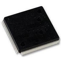
LFXP2-5E-5QN208C Lattice, LFXP2-5E-5QN208C Datasheet - Page 52

LFXP2-5E-5QN208C
Manufacturer Part Number
LFXP2-5E-5QN208C
Description
FPGA - Field Programmable Gate Array 5K LUTs 146I/O Inst- on DSP 1.2V -5 Spd
Manufacturer
Lattice
Datasheet
1.LFXP2-40E-5FN484I.pdf
(92 pages)
Specifications of LFXP2-5E-5QN208C
Number Of Macrocells
5000
Maximum Operating Frequency
200 MHz
Number Of Programmable I/os
146
Data Ram Size
10 KB
Supply Voltage (max)
1.14 V
Supply Current
17 mA
Maximum Operating Temperature
+ 85 C
Minimum Operating Temperature
0 C
Mounting Style
SMD/SMT
Supply Voltage (min)
1.26 V
Package / Case
PQFP-208
Lead Free Status / RoHS Status
Lead free / RoHS Compliant
Available stocks
Company
Part Number
Manufacturer
Quantity
Price
Company:
Part Number:
LFXP2-5E-5QN208C
Manufacturer:
Lattice Semiconductor Corporation
Quantity:
10 000
Part Number:
LFXP2-5E-5QN208C
Manufacturer:
LATTICE
Quantity:
20 000
Lattice Semiconductor
sysIO Differential Electrical Characteristics
LVDS
Differential HSTL and SSTL
Differential HSTL and SSTL outputs are implemented as a pair of complementary single-ended outputs. All allow-
able single-ended output classes (class I and class II) are supported in this mode.
For further information on LVPECL, RSDS, MLVDS, BLVDS and other differential interfaces please see details in
additional technical notes listed at the end of this data sheet.
LVDS25E
The top and bottom sides of LatticeXP2 devices support LVDS outputs via emulated complementary LVCMOS out-
puts in conjunction with a parallel resistor across the driver outputs. The scheme shown in Figure 3-1 is one possi-
ble solution for point-to-point signals.
Figure 3-1. LVDS25E Output Termination Example
V
V
V
I
V
V
V
V
V
V
I
I
Parameter
IN
SA
SAB
OH
OL
OD
OS
INP
CM
THD
OD
OS
, V
INM
Input Voltage
Input Common Mode Voltage
Differential Input Threshold
Input Current
Output High Voltage for V
Output Low Voltage for V
Output Voltage Differential
Change in V
Low
Output Voltage Offset
Change in V
Output Short Circuit Current
Output Short Circuit Current
VCCIO = 2.5V (±5%)
VCCIO = 2.5V (±5%)
8 mA
8 mA
Description
OD
OS
Between H and L
Between High and
ON-chip
OFF-chip
Over Recommended Operating Conditions
OP
OP
or V
or V
RS=158 ohms
(±1%)
RS=158 ohms
(±1%)
OM
OM
Transmission line, Zo = 100 ohm differential
Half the Sum of the Two Inputs
Power On or Power Off
R
R
(V
(V
V
Ground
V
Each Other
Difference Between the Two Inputs
OD
OD
T
T
OP
OP
= 100 Ohm
= 100 Ohm
= 0V Driver Outputs Shorted to
= 0V Driver Outputs Shorted to
- V
+ V
OM
OM
RP = 140 ohms
(±1%)
3-8
Test Conditions
), R
)/2, R
T
= 100 Ohm
T
= 100 Ohm
DC and Switching Characteristics
RT = 100 ohms
(±1%)
LatticeXP2 Family Data Sheet
OFF-chip ON-chip
+/-100
1.125
0.9V
Min.
0.05
250
—
—
—
—
—
—
0
Typ.
1.38
1.03
1.20
350
—
—
—
—
—
—
—
—
+
-
1.375
Max.
+/-10
2.35
1.60
450
2.4
50
50
24
12
—
—
Units
mV
mV
mV
mV
mA
mA
µA
V
V
V
V
V


