LFXP2-5E-5QN208C Lattice, LFXP2-5E-5QN208C Datasheet - Page 13
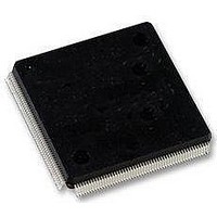
LFXP2-5E-5QN208C
Manufacturer Part Number
LFXP2-5E-5QN208C
Description
FPGA - Field Programmable Gate Array 5K LUTs 146I/O Inst- on DSP 1.2V -5 Spd
Manufacturer
Lattice
Datasheet
1.LFXP2-40E-5FN484I.pdf
(92 pages)
Specifications of LFXP2-5E-5QN208C
Number Of Macrocells
5000
Maximum Operating Frequency
200 MHz
Number Of Programmable I/os
146
Data Ram Size
10 KB
Supply Voltage (max)
1.14 V
Supply Current
17 mA
Maximum Operating Temperature
+ 85 C
Minimum Operating Temperature
0 C
Mounting Style
SMD/SMT
Supply Voltage (min)
1.26 V
Package / Case
PQFP-208
Lead Free Status / RoHS Status
Lead free / RoHS Compliant
Available stocks
Company
Part Number
Manufacturer
Quantity
Price
Company:

Part Number:
LFXP2-5E-5QN208C
Manufacturer:
Lattice Semiconductor Corporation
Quantity:
10 000
Part Number:
LFXP2-5E-5QN208C
Manufacturer:
LATTICE
Quantity:
20 000


Lattice Semiconductor
Secondary Clock/Control Sources
LatticeXP2 devices derive secondary clocks (SC0 through SC7) from eight dedicated clock input pads and the rest
from routing. Figure 2-7 shows the secondary clock sources.
Figure 2-7. Secondary Clock Sources
Clock Input
Clock Input
From Routing
From Routing
From Routing
From Routing
Routing
Routing
From
From
Routing
Routing
From
From
Secondary Clock Sources
Clock
Clock
Input
Input
2-10
Clock
Clock
Input
Input
Routing
Routing
From
From
LatticeXP2 Family Data Sheet
Routing
Routing
From
From
From Routing
From Routing
From Routing
From Routing
Clock Input
Clock Input
Architecture
Related parts for LFXP2-5E-5QN208C
Image
Part Number
Description
Manufacturer
Datasheet
Request
R

Part Number:
Description:
FPGA - Field Programmable Gate Array 5K LUTs 172I/O Inst- on DSP 1.2V -5 Spd
Manufacturer:
Lattice
Datasheet:

Part Number:
Description:
FPGA - Field Programmable Gate Array 5K LUTs 172 I/O Inst on DSP 1.2V -5 Spd
Manufacturer:
Lattice
Datasheet:

Part Number:
Description:
FPGA - Field Programmable Gate Array 5K LUTs 100 I/O Inst on DSP 1.2V -5 Spd
Manufacturer:
Lattice
Datasheet:

Part Number:
Description:
FPGA - Field Programmable Gate Array 5K LUTs 100I/O Inst- on DSP 1.2V -5 Spd
Manufacturer:
Lattice
Datasheet:

Part Number:
Description:
FPGA LatticeXP2 Family 5000 Cells Flash Technology 1.2V 256-Pin FTBGA
Manufacturer:
LATTICE SEMICONDUCTOR
Datasheet:
Part Number:
Description:
FPGA LatticeXP2 Family 5000 Cells Flash Technology 1.2V 256-Pin FTBGA
Manufacturer:
LATTICE SEMICONDUCTOR
Datasheet:
Part Number:
Description:
IC DSP 5KLUTS 100I/O 144TQFP
Manufacturer:
Lattice
Datasheet:
Part Number:
Description:
IC DSP 5KLUTS 86I/O 132CSBGA
Manufacturer:
Lattice
Datasheet:
Part Number:
Description:
IC DSP 5KLUTS 86I/O 132CSBGA
Manufacturer:
Lattice
Datasheet:
Part Number:
Description:
IC DSP 5KLUTS 146I/O 208PQFP
Manufacturer:
Lattice
Datasheet:
Part Number:
Description:
IC DSP 5KLUTS 146I/O 208PQFP
Manufacturer:
Lattice
Datasheet:
Part Number:
Description:
IC DSP 5KLUTS 172I/O 256FTBGA
Manufacturer:
Lattice
Datasheet:
Part Number:
Description:
IC FPGA 5KLUTS 86I/O 132-BGA
Manufacturer:
Lattice
Datasheet:
Part Number:
Description:
IC FPGA 5KLUTS 86I/O 132-BGA
Manufacturer:
Lattice
Datasheet:
Part Number:
Description:
IC FPGA 5KLUTS 86I/O 132-BGA
Manufacturer:
Lattice
Datasheet: