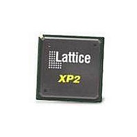
LFXP2-8E-5TN144C Lattice, LFXP2-8E-5TN144C Datasheet - Page 17

LFXP2-8E-5TN144C
Manufacturer Part Number
LFXP2-8E-5TN144C
Description
FPGA - Field Programmable Gate Array 8K LUTs 100I/O Inst- on DSP 1.2V -5 Spd
Manufacturer
Lattice
Series
LatticeXP2r
Datasheet
1.LFXP2-40E-5FN484I.pdf
(92 pages)
Specifications of LFXP2-8E-5TN144C
Number Of Macrocells
8000
Number Of Programmable I/os
100
Data Ram Size
226304
Supply Voltage (max)
1.26 V
Maximum Operating Temperature
+ 85 C
Minimum Operating Temperature
0 C
Mounting Style
SMD/SMT
Supply Voltage (min)
1.14 V
Package / Case
TQFP-144
No. Of Logic Blocks
8000
No. Of Macrocells
4000
Family Type
LatticeXP2
No. Of Speed Grades
5
Total Ram Bits
221Kbit
No. Of I/o's
100
Clock Management
PLL
Rohs Compliant
Yes
Lead Free Status / RoHS Status
Lead free / RoHS Compliant
Available stocks
Company
Part Number
Manufacturer
Quantity
Price
Company:
Part Number:
LFXP2-8E-5TN144C
Manufacturer:
Lattice Semiconductor Corporation
Quantity:
10 000
Part Number:
LFXP2-8E-5TN144C
Manufacturer:
LATTICE
Quantity:
20 000
Lattice Semiconductor
Figure 2-12. Secondary Clock Selection
Slice Clock Selection
Figure 2-13 shows the clock selections and Figure 2-14 shows the control selections for Slice0 through Slice2. All
the primary clocks and the four secondary clocks are routed to this clock selection mux. Other signals, via routing,
can be used as clock inputs to the slices. Slice controls are generated from the secondary clocks or other signals
connected via routing.
If none of the signals are selected for both clock and control, then the default value of the mux output is 1. Slice 3
does not have any registers; therefore it does not have the clock or control muxes.
Figure 2-13. Slice0 through Slice2 Clock Selection
4 Secondary Clocks/CE/LSR (SC0 to SC3) per Region
SC0
24:1
Secondary Clock
Primary Clock
SC1
24:1
Clock/Control
Routing
Secondary Clock Feedlines: 8 PIOs + 16 Routing
SC2
Vcc
24:1
SC3
12
24:1
8
4
1
4 High Fan-out Data Signals (SC4 to SC7) per Region
2-14
SC4
24:1
25:1
SC5
High Fan-out Data
24:1
Clock to Slice
SC6
LatticeXP2 Family Data Sheet
24:1
SC7
24:1
Architecture


