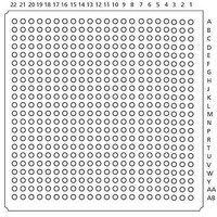
AGL400V5-FGG484 Actel, AGL400V5-FGG484 Datasheet - Page 100
AGL400V5-FGG484
Manufacturer Part Number
AGL400V5-FGG484
Description
FPGA - Field Programmable Gate Array 400K System Gates
Manufacturer
Actel
Datasheet
1.AGL030V2-CSG81.pdf
(236 pages)
Specifications of AGL400V5-FGG484
Processor Series
AGL400
Core
IP Core
Number Of Logic Blocks
12
Maximum Operating Frequency
250 MHz
Number Of Programmable I/os
194
Data Ram Size
54 Kbit
Supply Voltage (max)
1.5 V
Supply Current
27 uA
Maximum Operating Temperature
+ 70 C
Minimum Operating Temperature
0 C
Development Tools By Supplier
AGL-Icicle-Kit, AGL-Dev-Kit-SCS, Silicon-Explorer II, Silicon-Sculptor 3, SI-EX-TCA, FlashPro 4, FlashPro 3, FlashPro Lite
Mounting Style
SMD/SMT
Supply Voltage (min)
1.425 V
Number Of Gates
400 K
Package / Case
FPBGA-484
Lead Free Status / RoHS Status
Lead free / RoHS Compliant
Available stocks
Company
Part Number
Manufacturer
Quantity
Price
Company:

Part Number:
AGL400V5-FGG484
Manufacturer:
Actel
Quantity:
135
Company:
Part Number:
AGL400V5-FGG484
Manufacturer:
Microsemi SoC
Quantity:
10 000
Company:
Part Number:
AGL400V5-FGG484I
Manufacturer:
Microsemi SoC
Quantity:
10 000


IGLOO DC and Switching Characteristics
Table 2-154 • Parameter Definition and Measuring Nodes
2- 86
Parameter Name
t
t
t
t
t
t
t
t
t
t
t
t
t
t
t
t
t
t
t
t
t
t
t
t
Note:
OCLKQ
OSUD
OHD
OSUE
OHE
OPRE2Q
OREMPRE
ORECPRE
OECLKQ
OESUD
OEHD
OESUE
OEHE
OEPRE2Q
OEREMPRE
OERECPRE
ICLKQ
ISUD
IHD
ISUE
IHE
IPRE2Q
IREMPRE
IRECPRE
*See
Figure 2-16 on page 2-85
Clock-to-Q of the Output Data Register
Data Setup Time for the Output Data Register
Data Hold Time for the Output Data Register
Enable Setup Time for the Output Data Register
Enable Hold Time for the Output Data Register
Asynchronous Preset-to-Q of the Output Data Register
Asynchronous Preset Removal Time for the Output Data Register
Asynchronous Preset Recovery Time for the Output Data Register
Clock-to-Q of the Output Enable Register
Data Setup Time for the Output Enable Register
Data Hold Time for the Output Enable Register
Enable Setup Time for the Output Enable Register
Enable Hold Time for the Output Enable Register
Asynchronous Preset-to-Q of the Output Enable Register
Asynchronous Preset Removal Time for the Output Enable Register
Asynchronous Preset Recovery Time for the Output Enable Register
Clock-to-Q of the Input Data Register
Data Setup Time for the Input Data Register
Data Hold Time for the Input Data Register
Enable Setup Time for the Input Data Register
Enable Hold Time for the Input Data Register
Asynchronous Preset-to-Q of the Input Data Register
Asynchronous Preset Removal Time for the Input Data Register
Asynchronous Preset Recovery Time for the Input Data Register
for more information.
Parameter Definition
R ev i sio n 1 8
Measuring Nodes
(from, to)*
H, DOUT
H, EOUT
L, DOUT
I, EOUT
G, H
G, H
K, H
K, H
C, A
C, A
D, E
D, A
F, H
L, H
L, H
J, H
A, E
B, A
B, A
D, A
F, H
J, H
I, H
I, H
Related parts for AGL400V5-FGG484
Image
Part Number
Description
Manufacturer
Datasheet
Request
R

Part Number:
Description:
PBGA 196/FPGA, 9216 CLBS, 400000 GATES
Manufacturer:
Actel

Part Number:
Description:
FPGA - Field Programmable Gate Array 400K System Gates
Manufacturer:
Actel
Datasheet:

Part Number:
Description:
FPGA - Field Programmable Gate Array 400K System Gates
Manufacturer:
Actel
Datasheet:
Part Number:
Description:
FPGA - Field Programmable Gate Array 400K System Gates
Manufacturer:
Actel
Datasheet:

Part Number:
Description:
FPGA - Field Programmable Gate Array 400K System Gates
Manufacturer:
Actel
Datasheet:
Part Number:
Description:
MCU, MPU & DSP Development Tools Silicon Sculptor Programming Mod
Manufacturer:
Actel
Part Number:
Description:
MCU, MPU & DSP Development Tools InSystem Programming ProASICPLUS Devices
Manufacturer:
Actel
Part Number:
Description:
Programming Socket Adapters & Emulators PQ160 Module
Manufacturer:
Actel
Part Number:
Description:
Programming Socket Adapters & Emulators Axcelerator Adap Module Kit
Manufacturer:
Actel
Part Number:
Description:
Programming Socket Adapters & Emulators Evaluation
Manufacturer:
Actel