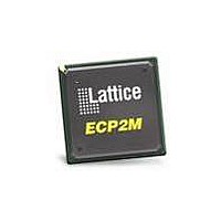
LFE2M20E-6FN484C Lattice, LFE2M20E-6FN484C Datasheet - Page 16

LFE2M20E-6FN484C
Manufacturer Part Number
LFE2M20E-6FN484C
Description
FPGA - Field Programmable Gate Array 19K LUTs 304 I/O SERDES DSP -6
Manufacturer
Lattice
Datasheet
1.LFE2-12SE-6FN256C.pdf
(389 pages)
Specifications of LFE2M20E-6FN484C
Number Of Macrocells
19000
Maximum Operating Frequency
357 MHz
Number Of Programmable I/os
304
Data Ram Size
1246208
Supply Voltage (max)
1.26 V
Maximum Operating Temperature
+ 85 C
Minimum Operating Temperature
0 C
Mounting Style
SMD/SMT
Supply Voltage (min)
1.14 V
Package / Case
FPBGA-484
Lead Free Status / RoHS Status
Lead free / RoHS Compliant
Available stocks
Company
Part Number
Manufacturer
Quantity
Price
Company:
Part Number:
LFE2M20E-6FN484C
Manufacturer:
Lattice
Quantity:
135
Company:
Part Number:
LFE2M20E-6FN484C
Manufacturer:
LATTICE
Quantity:
350
Company:
Part Number:
LFE2M20E-6FN484C
Manufacturer:
Lattice Semiconductor Corporation
Quantity:
10 000
Company:
Part Number:
LFE2M20E-6FN484C-5I
Manufacturer:
LATTICE
Quantity:
11
Part Number:
LFE2M20E-6FN484C-5I
Manufacturer:
LATTICE
Quantity:
20 000
- Current page: 16 of 389
- Download datasheet (5Mb)
Lattice Semiconductor
Secondary Clock/Control Sources
LatticeECP2/M devices derive secondary clocks (SC0 through SC7) from eight dedicated clock input pads and the
rest from routing. Figure 2-11 shows the secondary clock sources.
Figure 2-11. Secondary Clock Sources
Clock Input
Clock Input
From Routing
From Routing
From Routing
From Routing
Routing
Routing
From
From
Routing
Routing
From
From
Secondary Clock Sources
Clock
Clock
Input
Input
2-13
Clock
Clock
Input
Input
Routing
Routing
From
From
LatticeECP2/M Family Data Sheet
Routing
Routing
From
From
From Routing
From Routing
From Routing
From Routing
Clock Input
Clock Input
Architecture
Related parts for LFE2M20E-6FN484C
Image
Part Number
Description
Manufacturer
Datasheet
Request
R

Part Number:
Description:
FPGA - Field Programmable Gate Array 19K LUTs 140 I/O SERDES DSP -6
Manufacturer:
Lattice
Datasheet:

Part Number:
Description:
FPGA - Field Programmable Gate Array 19K LUTs 304 I/O SERDES DSP -6 I
Manufacturer:
Lattice

Part Number:
Description:
FPGA - Field Programmable Gate Array 19K LUTs 140 I/O SERDES DSP -6 I
Manufacturer:
Lattice

Part Number:
Description:
FPGA - Field Programmable Gate Array 19K LUTs 304 I/O SERDES DSP -6
Manufacturer:
Lattice

Part Number:
Description:
FPGA - Field Programmable Gate Array 19K LUTs 304 I/O SERDES DSP -5
Manufacturer:
Lattice
Datasheet:

Part Number:
Description:
FPGA - Field Programmable Gate Array 19K LUTs 140 I/O SERDES DSP -5
Manufacturer:
Lattice
Datasheet:
Part Number:
Description:
FPGA LatticeECP2M Family 19000 Cells 90nm (CMOS) Technology 1.2V 484-Pin FBGA
Manufacturer:
LATTICE SEMICONDUCTOR
Datasheet:
Part Number:
Description:
FPGA LatticeECP2M Family 19000 Cells 90nm (CMOS) Technology 1.2V 256-Pin FBGA
Manufacturer:
LATTICE SEMICONDUCTOR
Datasheet:
Part Number:
Description:
FPGA LatticeECP2M Family 19000 Cells 90nm (CMOS) Technology 1.2V 256-Pin FBGA
Manufacturer:
LATTICE SEMICONDUCTOR
Datasheet:

Part Number:
Description:
IC FPGA 20KLUTS 140I/O 256-BGA
Manufacturer:
Lattice
Datasheet:

Part Number:
Description:
IC FPGA 20KLUTS 140I/O 256-BGA
Manufacturer:
Lattice
Datasheet:

Part Number:
Description:
IC FPGA 20KLUTS 140I/O 256-BGA
Manufacturer:
Lattice
Datasheet:

Part Number:
Description:
IC FPGA 20KLUTS 304I/O 484-BGA
Manufacturer:
Lattice
Datasheet:

Part Number:
Description:
IC FPGA 20KLUTS 140I/O 256-BGA
Manufacturer:
Lattice
Datasheet:


