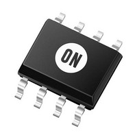
NCP3126ADR2G ON Semiconductor, NCP3126ADR2G Datasheet - Page 3

NCP3126ADR2G
Manufacturer Part Number
NCP3126ADR2G
Description
DC/DC Switching Converters 3A PWM Switching Buck Regulator
Manufacturer
ON Semiconductor
Datasheet
1.NCP3126ADR2G.pdf
(23 pages)
Specifications of NCP3126ADR2G
Mounting Style
SMD/SMT
Duty Cycle (max)
80 %
Efficiency
93 %
Input / Supply Voltage (max)
13.2 V
Input / Supply Voltage (min)
4.5 V
Maximum Operating Temperature
+ 125 C
Minimum Operating Temperature
- 40 C
Operating Temperature Range
- 40 C to + 125 C
Output Current
3 A
Output Voltage
Adjustable
Supply Current
10 mA
Switching Frequency
350 KHz
Package / Case
SOIC-8
Lead Free Status / RoHS Status
Lead free / RoHS Compliant
Available stocks
Company
Part Number
Manufacturer
Quantity
Price
Company:
Part Number:
NCP3126ADR2G
Manufacturer:
ON
Quantity:
2 500
Stresses exceeding Maximum Ratings may damage the device. Maximum Ratings are stress ratings only. Functional operation above the
Recommended Operating Conditions is not implied. Extended exposure to stresses above the Recommended Operating Conditions may affect
device reliability.
1. The maximum package power dissipation limit must not be exceeded.
2. The value of qJA is measured with the device mounted on 1 in
3. The value of qJA is measured with the device mounted on minimum footprint, in a still air environment with T
4. 60−180 seconds minimum above 237°C.
Table 2. MAXIMUM RATINGS
Main Supply Voltage Input
Bootstrap Supply Voltage vs GND
Bootstrap Supply Voltage vs Ground (spikes ≤ 50 ns)
Bootstrap Pin Voltage vs V
High Side Switch Max DC Current
V
Switching Node Voltage Excursion (200 mA)
Switch Pin voltage (spikes < 50 ns)
FB Pin Voltage
COMP/DISABLE
Low Side Driver Pin Voltage
Low Side Driver Pin Voltage (spikes v 200 ns)
Thermal Resistance, Junction−to−Ambient
Thermal Resistance, Junction−to−Case
Storage Temperature Range
Junction Operating Temperature
Lead Temperature Soldering (10 sec):
Reflow (SMD styles only) Pb−Free
value in any given application depends on the user’s specific board design.
application depends on the user’s specific board design.
SW
Pin Voltage
SW
Rating
Rating
(Note 2)
(Note 3)
http://onsemi.com
2
FR−4 board with 1 oz. copper, in a still air environment with T
3
VCOMP/DIS
VISET Spike
VBST spike
VBST−V
Symbol
Symbol
V
VISET
VBST
V
IV
R
R
V
SWLIM
VFB
T
V
RF
SWtr
T
SW
qJA
qJC
stg
SW
IN
J
SW
−0.3
−0.3
−5.0
−0.3
−0.3
−2.0
−5.0
−0.3
−0.3
−0.3
Min
−2
0
−55 to 150
−40 to 125
260 peak
Rating
A
183
170
110
= 25°C. The value in any given
5.5 < V
5.5 < V
15 < V
15 < V
Max
3.0
15
15
35
15
30
35
40
CC
CC
CC
CC
A
= 25°C. The
°C/W
°C/W
Unit
Unit
°C
°C
°C
V
V
V
V
A
V
V
V
V
V
V
V


