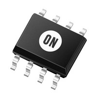
NCP3126ADR2G ON Semiconductor, NCP3126ADR2G Datasheet - Page 14

NCP3126ADR2G
Manufacturer Part Number
NCP3126ADR2G
Description
DC/DC Switching Converters 3A PWM Switching Buck Regulator
Manufacturer
ON Semiconductor
Datasheet
1.NCP3126ADR2G.pdf
(23 pages)
Specifications of NCP3126ADR2G
Mounting Style
SMD/SMT
Duty Cycle (max)
80 %
Efficiency
93 %
Input / Supply Voltage (max)
13.2 V
Input / Supply Voltage (min)
4.5 V
Maximum Operating Temperature
+ 125 C
Minimum Operating Temperature
- 40 C
Operating Temperature Range
- 40 C to + 125 C
Output Current
3 A
Output Voltage
Adjustable
Supply Current
10 mA
Switching Frequency
350 KHz
Package / Case
SOIC-8
Lead Free Status / RoHS Status
Lead free / RoHS Compliant
Available stocks
Company
Part Number
Manufacturer
Quantity
Price
Company:
Part Number:
NCP3126ADR2G
Manufacturer:
ON
Quantity:
2 500
ambient temperature. The formula for calculating the
junction temperature with the package in free air is:
P
R
T
T
should be performed to ensure the design will dissipate the
required power under worst case operating conditions.
Variables considered during testing should include
maximum ambient temperature, minimum airflow,
maximum input voltage, maximum loading, and component
variations (i.e., worst case MOSFET R
Compensation Network
network around the transconductance amplifier must be
used in conjunction with the PWM generator and the power
stage. Since the power stage design criteria is set by the
application, the compensation network must correct the over
all system response to ensure stability. The output inductor
and capacitor of the power stage form a double pole at the
frequency as shown in Equation 36:
C
F
L
frequency as shown in Equation 37:
CO
C
F
power stage has created or open loop response of the system.
The next step is to close the loop by considering the feedback
values. The closed loop crossover frequency should be
greater than the F
frequency, which would place the maximum crossover
frequency at 70 kHz. Further, the calculated F
should meet the following:
D
A
LC
LC
J
OUT
qJA
OUT
OUT
As with any power design, proper laboratory testing
To create a stable power supply, the compensation
The ESR of the output capacitor creates a “zero” at the
The two equations above define the bode plot that the
2.773 kHz +
ESR
2.85 kHz +
F
F
LC
ESR
+
= Power dissipation of the IC
= Thermal resistance junction to ambient of
= Ambient temperature
= Junction temperature
= Output capacitor
= Double pole inductor and capacitor
= Output inductor value
+
= Output capacitor ESR
= Output capacitor
= Output capacitor ESR frequency
2p L
2p
the regulator package
frequency
2p
2p
T
LC
J
+ T
OUT
and less than 1/5 of the switching
CO
F
0.050 mW
1
ESR
6.8 mH
A
ESR
1
) P
C
t
1
1
OUT
F
D
SW
5
C
@ R
³
470 mF
OUT
470 mF
qJA
DS(on)
³
ESR
).
frequency
(eq. 35)
(eq. 36)
(eq. 37)
(eq. 38)
http://onsemi.com
14
F
F
not provide stability and the output power stage must be
modified.
amplifier.
and the impedance networks Z
external Z
has to provide a closed loop transfer function with the
highest 0 dB crossing frequency to have fast response and
the highest gain in DC conditions to minimize the load
regulation issues. A stable control loop has a gain crossing
with −20 dB/decade slope and a phase margin greater than
45°. Include worst−case component variations when
determining phase margin. To start the design, a resistor
value should be chosen for R
components can be chosen. A good starting value is 10 kW.
to be adjusted down to 0.8 V via an external resistor divider
network. The regulator will maintain 0.8 V at the feedback
pin. Thus, if a resistor divider circuit was placed across the
feedback pin to V
voltage proportional to the resistor divider network in order
to maintain 0.8 V at the FB pin.
above and the output voltage is shown in Equation 39:
SW
ESR
Figure 23. Pseudo Type III Transconductance Error
If the criteria is not met, the compensation network may
Figure 23 shows a pseudo Type III transconductance error
The compensation network consists of the internal OTA
The NCP3126 allows the output of the DC−DC regulator
The relationship between the resistor divider network
RC
CC
ZFB
Figure 24. Feedback Resistor Divider
FB
(R
CP
C
, C
OUT
= Switching frequency
= Output capacitor ESR zero frequency
C
, and C
, the regulator will regulate the output
R1
R2
V
Amplifier
OUT
P
Gm
IEA
). The compensation network
VREF
FB
IN
2
(R
from which all other
1
, R
2
, R
R 1
F
, and C
ZIN
R 2
F
CF
RF
) and


