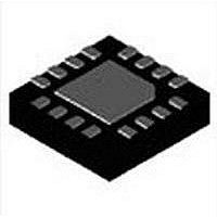
MAX5974CETE+ Maxim Integrated Products, MAX5974CETE+ Datasheet - Page 21

MAX5974CETE+
Manufacturer Part Number
MAX5974CETE+
Description
Current Mode PWM Controllers ACTIVE-CLAMPED CUR MODE PWM CONTLR
Manufacturer
Maxim Integrated Products
Datasheet
1.MAX5974DETE.pdf
(26 pages)
Specifications of MAX5974CETE+
Duty Cycle (max)
82 %
Mounting Style
SMD/SMT
Switching Frequency
600 KHz
Operating Supply Voltage
12 V to 21 V
Supply Current
1.8 mA
Maximum Operating Temperature
+ 85 C
Fall Time
14 ns
Minimum Operating Temperature
- 40 C
Rise Time
27 ns
Package / Case
TQFN-16
Lead Free Status / RoHS Status
Lead free / RoHS Compliant
Traditional clamp circuits prevent transformer saturation
by channeling the magnetizing current (I
former onto a dissipative RC network. To improve effi-
ciency, the active clamp circuit recycles I
magnetizing inductance and clamp capacitor. V
is given by:
where V
the duty cycle. To select n-channel and p-channel FETs
with adequate breakdown voltages, use the maximum
value of V
voltage is at its minimum and the duty cycle is at its
maximum. V
tion is therefore:
where V
source, N
and V
n-channel, and p-channel FETs must have breakdown
voltages exceeding this level.
If feed-forward maximum duty-cycle clamp is used then:
Therefore, V
mum duty clamp is:
The AUX driver controls the p-channel FET through a
level shifter. The level shifter consists of an RC network
O
V
S
CLAMP(MAX-NORMAL)
S(MIN)
is the output voltage. The clamp capacitor,
P
CLAMP
is the voltage of the power source and D is
=
/N
D
V
CLAMP(MAX-NORMAL)
CLAMP(MAX-FF)
=
MAX-FF
1
S
CLAMP(MAX-FF)
2.43
−
is the primary to secondary turns ratio,
is the minimum voltage of the power
2.43 R
. V
V
S
×
CLAMP(MAX)
V
(
=
×
R
CLAMP
DCLMP1
V
2.43
R
MIN
DCLMP1
DCLMP2
R
=
during feed-forward maxi-
=
=
Active Clamp Circuit
DCLMP2
=
1 D
1 D
+
1
Active-Clamped, Spread-Spectrum,
V
−
−
1
+
−
R
occurs when the input
S
−
R
DCLMP2
during normal opera-
V
N
MAX FF
DCLMP2
DCLMP
V
V
2.43
S
S
N
S(MIN)
×
P
−
V
M
×
M
Current-Mode PWM Controllers
S(MIN)
) of the trans-
)
V
between the
O
CLAMP
(formed by C
in the Typical Application Circuits. Choose R
C
D5 is a small-signal diode with a voltage rating exceed-
ing 25V.
Additionally, C
complex poles formed with magnetizing inductance
(L
bandwidth:
An in-phase tertiary winding is needed to power the bias
circuit when using optocoupler feedback. The voltage
across the tertiary V
where V
ratio from the tertiary to the secondary winding. Select the
turns ratio so that V
(7.5V max) by a margin determined by the holdup time
needed to “ride through” a brownout.
When using coupled-inductor feedback, the power for
the devices can be taken from the coupled inductor dur-
ing the off-time. The voltage across the coupled induc-
tor, V
where V
turns ratio from the coupled output to the main output
winding. Select the turns ratio so that V
above the UVLO shutdown level (7.5V max) by a margin
determined by the holdup time needed to “ride through”
a brownout.
This voltage appears at the input of the devices, less
a diode drop. An RC network consisting of R
C
diode D6.
Coupled-Inductor Feedback (MAX5974A/MAX5974B)
AUX
SNUB
MAG
COUPLED
Optocoupler Feedback (MAX5974C/MAX5974D)
so that the time constant exceeds 100/f
) and C
is for damping the reverse recovery transients of
OUT
OUT
is the output voltage and N
2
AUX
is the output voltage and N
π
CLAMP
, during the off-time is:
CLAMP
V
L
COUPLED
MAG
and R
T
V
T
T
1-D
is above the UVLO shutdown level
during the on-time is:
are 2x to 4x away from the loop
should be chosen such that the
=
×
AUX
C
V
OUT
CLAMP
=
) and diode D5, as shown
V
OUT
×
N
N
> ×
T
S
×
3 f
N
N
C
O
T
BW
/N
Bias Circuit
S
C
COUPLED
is the turns
/N
SW
SNUB
AUX
O
. Diode
is the
and
and
21
is


