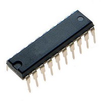
ATTINY461V-10PU Atmel, ATTINY461V-10PU Datasheet - Page 156
ATTINY461V-10PU
Manufacturer Part Number
ATTINY461V-10PU
Description
Microcontrollers (MCU) 4kB Flash 0.256kB EEPROM 16 I/O Pins
Manufacturer
Atmel
Specifications of ATTINY461V-10PU
Processor Series
ATTINY4x
Core
AVR8
Data Bus Width
8 bit
Data Ram Size
256 B
Interface Type
2-Wire/SPI/USI
Maximum Clock Frequency
10 MHz
Number Of Programmable I/os
16
Number Of Timers
2
Operating Supply Voltage
2.7 V to 5.5 V
Maximum Operating Temperature
+ 85 C
Mounting Style
Through Hole
Minimum Operating Temperature
- 40 C
On-chip Adc
11-ch x 10-bit
Program Memory Type
Flash
Program Memory Size
4 KB
Package / Case
PDIP-20
Package
20PDIP
Device Core
AVR
Family Name
ATtiny
Maximum Speed
10 MHz
Ram Size
256 Byte
Operating Temperature
-40 to 85 °C
Lead Free Status / RoHS Status
Lead free / RoHS Compliant
Available stocks
Company
Part Number
Manufacturer
Quantity
Price
Company:

Part Number:
ATTINY461V-10PU
Manufacturer:
ATMEL
Quantity:
6 223


Special care should be taken when changing differential channels. Once a differential channel
has been selected the input stage may take a while to stabilize. It is therefore recommended to
force the ADC to perform a long conversion when changing multiplexer or voltage reference set-
tings. This can be done by first turning off the ADC, then changing reference settings and then
turn on the ADC. Alternatively, the first conversion results after changing reference settings
should be discarded.
It is not recommended to use an external AREF higher than (V
- 1V) for channels with differ-
CC
ential gain, as this will affect ADC accuracy.
Internal voltage reference options may not be used if an external voltage is being applied to the
AREF pin.
• Bit 5 – ADLAR: ADC Left Adjust Result
The ADLAR bit affects the presentation of the ADC conversion result in the ADC Data Register.
Write one to ADLAR to left adjust the result. Otherwise, the result is right adjusted. Changing the
ADLAR bit will affect the ADC Data Register immediately, regardless of any ongoing conver-
sions. For a comple te description of this bit, see
“ADCL and ADCH – The ADC Data Register”
on page
160.
• Bits 4:0 – MUX4:0: Analog Channel and Gain Selection Bits
These bits and the MUX5 bit from the ADC Control and Status Register B (ADCSRB) select
which combination of analog inputs are connected to the ADC. In case of differential input, gain
selection is also made with these bits. Selecting the same pin as both inputs to the differential
ATtiny261/461/861
156
2588E–AVR–08/10
Related parts for ATTINY461V-10PU
Image
Part Number
Description
Manufacturer
Datasheet
Request
R

Part Number:
Description:
Manufacturer:
Atmel Corporation
Datasheet:
Part Number:
Description:
Manufacturer:
Atmel Corporation
Datasheet:

Part Number:
Description:
IC AVR MCU 4K 20MHZ 32-QFN
Manufacturer:
Atmel
Datasheet:

Part Number:
Description:
IC MCU AVR 4K FLASH 20MHZ 20SOIC
Manufacturer:
Atmel
Datasheet:

Part Number:
Description:
MCU AVR 4K FLASH 15MHZ 32-QFN
Manufacturer:
Atmel
Datasheet:
Part Number:
Description:
MCU AVR 4KB FLASH 15MHZ 32-VQFN
Manufacturer:
Atmel
Datasheet:
Part Number:
Description:
MCU AVR 4KB FLASH 20MHZ 20SOIC
Manufacturer:
Atmel
Datasheet:


Part Number:
Description:
IC MCU AVR 4K 20MHZ 32QFN
Manufacturer:
Atmel
Datasheet:

Part Number:
Description:
Microcontrollers (MCU) 4kB Flash 0.256kB EEPROM 16 I/O Pins
Manufacturer:
Atmel
Datasheet:
Part Number:
Description:
IC, MCU, 8BIT, 2K FLASH, 20SOIC
Manufacturer:
Atmel
Datasheet: