PCA9554PW/DG,118 NXP Semiconductors, PCA9554PW/DG,118 Datasheet - Page 7

PCA9554PW/DG,118
Manufacturer Part Number
PCA9554PW/DG,118
Description
I/O Expanders, Repeaters & Hubs 8-BIT I2C FM TP GPIO
Manufacturer
NXP Semiconductors
Series
-r
Datasheet
1.PCA9554PWDG118.pdf
(30 pages)
Specifications of PCA9554PW/DG,118
Logic Family
PCA9554
Number Of Lines (input / Output)
8.0 / 8.0
Operating Supply Voltage
2.3 V to 5.5 V
Power Dissipation
200 mW
Operating Temperature Range
- 40 C to + 85 C
Input Voltage
5 V
Logic Type
I2C, SMBus
Maximum Clock Frequency
400 KHz
Mounting Style
SMD/SMT
Number Of Input Lines
8.0
Number Of Output Lines
8.0
Output Current
50 mA
Output Voltage
5 V
Package / Case
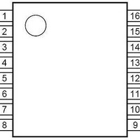
TSSOP-16
Mounting Type
Surface Mount
Voltage - Supply
2.3 V ~ 5.5 V
Operating Temperature
-40°C ~ 85°C
Interface
I²C, SMBus
Number Of I /o
8
Frequency - Clock
400kHz
Interrupt Output
Yes
Includes
POR
Lead Free Status / RoHS Status
Lead free / RoHS Compliant
Lead Free Status / RoHS Status
Lead free / RoHS Compliant, Lead free / RoHS Compliant
Other names
935285896118 PCA9554PW/DG-T
NXP Semiconductors
PCA9554_9554A_7
Product data sheet
6.1.2 Register 0 - Input Port register
6.1.3 Register 1 - Output Port register
This register is a read-only port. It reflects the incoming logic levels of the pins, regardless
of whether the pin is defined as an input or an output by Register 3. Writes to this register
have no effect.
The default ‘X’ is determined by the externally applied logic level, normally ‘1’ when no
external signal externally applied because of the internal pull-up resistors.
Table 4.
This register reflects the outgoing logic levels of the pins defined as outputs by Register 3.
Bit values in this register have no effect on pins defined as inputs. Reads from this register
return the value that is in the flip-flop controlling the output selection, not the actual pin
value.
Table 5.
Legend: * default value.
Bit
7
6
5
4
3
2
1
0
Bit
7
6
5
4
3
2
1
0
Symbol
I7
I6
I5
I4
I3
I2
I1
I0
Symbol
O7
O6
O5
O4
O3
O2
O1
O0
Register 0 - Input Port register bit description
Register 1 - Output Port register bit description
Access
read only
read only
read only
read only
read only
read only
read only
read only
Access
R
R
R
R
R
R
R
R
Rev. 07 — 13 November 2006
Value
X
X
X
X
X
X
X
X
Value
1*
1*
1*
1*
1*
1*
1*
1*
8-bit I
Description
reflects outgoing logic levels of pins defined as
outputs by Register 3
Description
determined by externally applied logic level
2
PCA9554/PCA9554A
C-bus and SMBus I/O port with interrupt
© NXP B.V. 2006. All rights reserved.
7 of 30


