SUD40N10-25-E3 Vishay, SUD40N10-25-E3 Datasheet - Page 4
SUD40N10-25-E3
Manufacturer Part Number
SUD40N10-25-E3
Description
MOSFET Power 100V 40A 33W
Manufacturer
Vishay
Datasheet
1.SUD40N10-25-E3.pdf
(5 pages)
Specifications of SUD40N10-25-E3
Transistor Polarity
N-Channel
Minimum Operating Temperature
- 55 C
Configuration
Single
Resistance Drain-source Rds (on)
0.025 Ohm @ 10 V
Drain-source Breakdown Voltage
100 V
Gate-source Breakdown Voltage
+/- 20 V
Continuous Drain Current
40 A
Power Dissipation
3000 mW
Maximum Operating Temperature
+ 175 C
Mounting Style
SMD/SMT
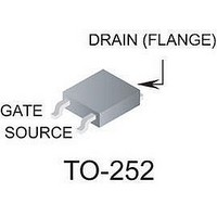
Package / Case
TO-252
Continuous Drain Current Id
40A
Drain Source Voltage Vds
100V
On Resistance Rds(on)
25mohm
Rds(on) Test Voltage Vgs
10V
Threshold Voltage Vgs Typ
3V
Lead Free Status / RoHS Status
Lead free / RoHS Compliant
Lead Free Status / RoHS Status
Lead free / RoHS Compliant, Lead free / RoHS Compliant
Available stocks
Company
Part Number
Manufacturer
Quantity
Price
Company:

Part Number:
SUD40N10-25-E3
Manufacturer:
VISHAY
Quantity:
12 000
Part Number:
SUD40N10-25-E3
Manufacturer:
VISHAY/威世
Quantity:
20 000


SUD40N10-25
Vishay Siliconix
TYPICAL CHARACTERISTICS 25 °C, unless otherwise noted
THERMAL RATINGS
Vishay Siliconix maintains worldwide manufacturing capability. Products may be manufactured at one of several qualified locations. Reliability data for Silicon
Technology and Package Reliability represent a composite of all qualified locations. For related documents such as package/tape drawings, part marking, and
reliability data, see
www.vishay.com
4
0.01
3.0
2.5
2.0
1.5
1.0
0.5
0.0
50
40
30
20
10
0.1
0
- 50 - 25
2
1
0
10
http://www.vishay.com/ppg?71140.
On-Resistance vs. Junction Temperature
V
I
0.1
-4
D
Duty Cycle = 0.5
0.2
GS
Maximum Avalanche Drain Current
= 40 A
25
= 10 V
Single Pulse
0
T
0.05
T
J
50
vs. Case Temperature
C
- Junction Temperature (
25
- Case Temperature (°C)
0.02
75
50
10
-3
75
100
Normalized Thermal Transient Impedance, Junction-to-Case
100
125
°C
125
)
150
150
10
-2
175
175
Square Wave Pulse Duration (s)
10
-1
100
100
0.1
10
10
1
1
0
0
1 .
Limited by R
* V
GS
Source-Drain Diode Forward Voltage
> minimum V
V
V
DS
0.3
SD
DS(on)
1
Single Pulse
- Drain-to-Source Voltage (V)
T
T
Safe Operating Area
- Source-to-Drain Voltage (V)
C
J
= 175 °C
= 25 °C
*
1
GS
at which R
1
0.6
S-81732-Rev. E, 04-Aug-08
0
Document Number: 71140
DS(on)
T
J
100
= 25 °C
0.9
is specified
10 µs
100 µs
1 ms
10 ms
100 ms
1 s, DC
10
1
0
1.2
0
30
0
Related parts for SUD40N10-25-E3
Image
Part Number
Description
Manufacturer
Datasheet
Request
R

Part Number:
Description:
N CHANNEL MOSFET, 100V, 30A, TO-252
Manufacturer:
Vishay
Datasheet:

Part Number:
Description:
357-036-542-201 CARDEDGE 36POS DL .156 BLK LOPRO
Manufacturer:
Vishay
Datasheet:
Part Number:
Description:
357-036-542-201 CARDEDGE 36POS DL .156 BLK LOPRO
Manufacturer:
Vishay
Datasheet:
Part Number:
Description:
357-036-542-201 CARDEDGE 36POS DL .156 BLK LOPRO
Manufacturer:
Vishay
Datasheet:
Part Number:
Description:
357-036-542-201 CARDEDGE 36POS DL .156 BLK LOPRO
Manufacturer:
Vishay
Datasheet:
Part Number:
Description:
357-036-542-201 CARDEDGE 36POS DL .156 BLK LOPRO
Manufacturer:
Vishay
Datasheet:
Part Number:
Description:
357-036-542-201 CARDEDGE 36POS DL .156 BLK LOPRO
Manufacturer:
Vishay
Datasheet:
Part Number:
Description:
357-036-542-201 CARDEDGE 36POS DL .156 BLK LOPRO
Manufacturer:
Vishay
Datasheet:
Part Number:
Description:
357-036-542-201 CARDEDGE 36POS DL .156 BLK LOPRO
Manufacturer:
Vishay
Datasheet:
Part Number:
Description:
357-036-542-201 CARDEDGE 36POS DL .156 BLK LOPRO
Manufacturer:
Vishay
Datasheet:
Part Number:
Description:
357-036-542-201 CARDEDGE 36POS DL .156 BLK LOPRO
Manufacturer:
Vishay
Datasheet:
Part Number:
Description:
357-036-542-201 CARDEDGE 36POS DL .156 BLK LOPRO
Manufacturer:
Vishay
Datasheet:
Part Number:
Description:
357-036-542-201 CARDEDGE 36POS DL .156 BLK LOPRO
Manufacturer:
Vishay
Datasheet:
Part Number:
Description:
357-036-542-201 CARDEDGE 36POS DL .156 BLK LOPRO
Manufacturer:
Vishay
Datasheet: