2N4392-E3 Vishay, 2N4392-E3 Datasheet - Page 3
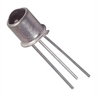
2N4392-E3
Manufacturer Part Number
2N4392-E3
Description
JFET 55V 5pA
Manufacturer
Vishay
Specifications of 2N4392-E3
Transistor Polarity
N-Channel
Configuration
Single
Power Dissipation
1800 mW
Package / Case
TO-206AA
Drain Source Voltage Vds
0.4 V
Gate-source Breakdown Voltage
- 40 V
Gate-source Cutoff Voltage
- 2 V to - 5 V
Drain Current (idss At Vgs=0)
25 mA to 75 mA
Forward Transconductance Gfs (max / Min)
6 mS
Resistance Drain-source Rds (on)
60 Ohms
Maximum Operating Temperature
+ 200 C
Maximum Drain Gate Voltage
- 40 V
Minimum Operating Temperature
- 55 C
Mounting Style
Through Hole
Breakdown Voltage Vbr
-55V
Gate-source Cutoff Voltage Vgs(off) Max
-5V
Power Dissipation Pd
1.8W
Operating Temperature Range
-55°C To +200°C
No. Of Pins
3
Channel Type
N
Gate-source Voltage (max)
-40V
Drain-gate Voltage (max)
-40V
Operating Temperature (min)
-55C
Operating Temperature Classification
Military
Mounting
Through Hole
Pin Count
3
Continuous Drain Current Id
25mA
Rohs Compliant
Yes
Transistor Type
JFET
Lead Free Status / RoHS Status
Lead free / RoHS Compliant
Lead Free Status / RoHS Status
Lead free / RoHS Compliant, Lead free / RoHS Compliant


Notes
a.
b.
Document Number: 70241
S-04028—Rev. F, 04-Jan-01
Dynamic
Common-Source
Forward Transconductance
Common-Source
Output Conductance
Drain-Source
On-Resistance
Common-Source
Input Capacitance
Input Capacitance
Common-Source
Reverse Transfer
Capacitance
Equivalent Input
Noise Voltage
Switching
Turn-On Time
Turn-Off Time
Typical values are for DESIGN AID ONLY, not guaranteed nor subject to production testing.
Pulse test: PW v300 ms duty cycle v3%.
Parameter
Symbol
r
DS(on)
t
t
C
C
d(on)
d(off)
g
g
e
t
rss
rss
t
os
iss
iss
fs
n
r
f
_
V
f = 1 MHz
f = 1 MHz
V
V
DS
V
See Switching Circuit
See Switching Circuit
DS
DS
GS
= 0 V
= 20 V, V
V
V
= 20 V, I
= 0 V, I
V
Test Conditions
f = 1 MHz
f = 1 MHz
DS
GS(H)
DD
= 10 V, I
= 10 V
= 0 V
D
f = 1 kHz
D
GS
= 0 mA , f = 1 kHz
= 1 mA, f = 1 kHz
SST: V
= 0 V
PN: V
2N: V
SST: V
SST: V
PN: V
PN: V
2N: V
2N: V
D
= 10 mA
GS
GS
GS
GS
GS
GS
GS
GS
GS
= –12 V
= –12 V
= –5 V
= –7 V
= –5 V
= –7 V
= –12 V
= –5 V
= –7 V
2N/PN
2N/PN
2N/PN
2N/PN
SST
SST
SST
SST
SST
2N
PN
Typ
3.3
3.2
2.8
3.5
3.4
3.0
3.6
3.5
3.1
25
12
12
13
13
13
6
3
2
2
2
2
6
6
a
Min
4391
2N/PN/SST4391 Series
Max
3.5
30
14
16
15
20
15
5
5
Min
Limits
4392
Max
Vishay Siliconix
3.5
60
14
16
15
35
20
5
5
Min
4393
Max
www.vishay.com
100
3.5
14
16
15
50
30
5
5
Unit
mS
nV
mS
pF
ns
W
Hz
NCB
7-3
Related parts for 2N4392-E3
Image
Part Number
Description
Manufacturer
Datasheet
Request
R


Part Number:
Description:
357-036-542-201 CARDEDGE 36POS DL .156 BLK LOPRO
Manufacturer:
Vishay
Datasheet:
Part Number:
Description:
357-036-542-201 CARDEDGE 36POS DL .156 BLK LOPRO
Manufacturer:
Vishay
Datasheet:
Part Number:
Description:
357-036-542-201 CARDEDGE 36POS DL .156 BLK LOPRO
Manufacturer:
Vishay
Datasheet:
Part Number:
Description:
357-036-542-201 CARDEDGE 36POS DL .156 BLK LOPRO
Manufacturer:
Vishay
Datasheet:
Part Number:
Description:
357-036-542-201 CARDEDGE 36POS DL .156 BLK LOPRO
Manufacturer:
Vishay
Datasheet:
Part Number:
Description:
357-036-542-201 CARDEDGE 36POS DL .156 BLK LOPRO
Manufacturer:
Vishay
Datasheet:
Part Number:
Description:
357-036-542-201 CARDEDGE 36POS DL .156 BLK LOPRO
Manufacturer:
Vishay
Datasheet:
Part Number:
Description:
357-036-542-201 CARDEDGE 36POS DL .156 BLK LOPRO
Manufacturer:
Vishay
Datasheet:
Part Number:
Description:
357-036-542-201 CARDEDGE 36POS DL .156 BLK LOPRO
Manufacturer:
Vishay
Datasheet:
Part Number:
Description:
357-036-542-201 CARDEDGE 36POS DL .156 BLK LOPRO
Manufacturer:
Vishay
Datasheet:
Part Number:
Description:
357-036-542-201 CARDEDGE 36POS DL .156 BLK LOPRO
Manufacturer:
Vishay
Datasheet:
Part Number:
Description:
357-036-542-201 CARDEDGE 36POS DL .156 BLK LOPRO
Manufacturer:
Vishay
Datasheet:
Part Number:
Description:
357-036-542-201 CARDEDGE 36POS DL .156 BLK LOPRO
Manufacturer:
Vishay
Datasheet: