PUMB11,115 NXP Semiconductors, PUMB11,115 Datasheet - Page 6
PUMB11,115
Manufacturer Part Number
PUMB11,115
Description
Digital Transistors / Resistor Biased TRNS DOUBL RET TAPE7
Manufacturer
NXP Semiconductors
Series
-r
Datasheet
1.PUMB11135.pdf
(8 pages)
Specifications of PUMB11,115
Configuration
Dual
Transistor Polarity
PNP
Typical Input Resistor
10 KOhm
Typical Resistor Ratio
1
Mounting Style
SMD/SMT
Package / Case
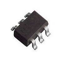
SOT-363
Collector- Emitter Voltage Vceo Max
50 V
Peak Dc Collector Current
100 mA
Maximum Operating Temperature
+ 150 C
Minimum Operating Temperature
- 65 C
Power - Max
300mW
Current - Collector (ic) (max)
100mA
Voltage - Collector Emitter Breakdown (max)
50V
Transistor Type
2 PNP - Pre-Biased (Dual)
Current - Collector Cutoff (max)
1µA
Dc Current Gain (hfe) (min) @ Ic, Vce
30 @ 5mA, 5V
Vce Saturation (max) @ Ib, Ic
150mV @ 500µA, 10mA
Resistor - Base (r1) (ohms)
10K
Resistor - Emitter Base (r2) (ohms)
10K
Frequency - Transition
-
Mounting Type
Surface Mount
Lead Free Status / RoHS Status
Lead free / RoHS Compliant
Frequency - Transition
-
Lead Free Status / Rohs Status
Lead free / RoHS Compliant
Other names
934056289115 PUMB11 T/R
Available stocks
Company
Part Number
Manufacturer
Quantity
Price

Part Number:
PUMB11,115
Manufacturer:
NEXPERIA/安世
Quantity:
20 000


NXP Semiconductors
2003 Oct 03
Plastic surface mounted package; 6 leads
PNP/PNP resistor-equipped transistors;
R1 = 10 kΩ, R2 = 10 kΩ
DIMENSIONS (mm are the original dimensions)
UNIT
mm
VERSION
OUTLINE
SOT363
1.1
0.8
A
max
0.1
A 1
1
6
0.30
0.20
b p
y
IEC
pin 1
index
e 1
0.25
0.10
c
D
e
2
5
2.2
1.8
b p
D
JEDEC
1.35
1.15
E
4
3
REFERENCES
0
1.3
e
w
B
M
B
0.65
e
1
SC-88
scale
EIAJ
6
1
H E
2.2
2.0
A
0.45
0.15
L p
A 1
2 mm
0.25
0.15
Q
H E
E
0.2
v
detail X
PROJECTION
0.2
EUROPEAN
w
PEMB11; PUMB11
L p
Q
0.1
A
y
c
Product data sheet
X
v
ISSUE DATE
M
97-02-28
A
SOT363
Related parts for PUMB11,115
Image
Part Number
Description
Manufacturer
Datasheet
Request
R

Part Number:
Description:
PNP Resistor-Equipped Double Transistor
Manufacturer:
Philips Semiconductors / NXP Semiconductors

Part Number:
Description:
TRANS ARRAY PNP/PNP SOT-363
Manufacturer:
NXP Semiconductors
Datasheet:

Part Number:
Description:
NXP Semiconductors designed the LPC2420/2460 microcontroller around a 16-bit/32-bitARM7TDMI-S CPU core with real-time debug interfaces that include both JTAG andembedded trace
Manufacturer:
NXP Semiconductors
Datasheet:

Part Number:
Description:
NXP Semiconductors designed the LPC2458 microcontroller around a 16-bit/32-bitARM7TDMI-S CPU core with real-time debug interfaces that include both JTAG andembedded trace
Manufacturer:
NXP Semiconductors
Datasheet:
Part Number:
Description:
NXP Semiconductors designed the LPC2468 microcontroller around a 16-bit/32-bitARM7TDMI-S CPU core with real-time debug interfaces that include both JTAG andembedded trace
Manufacturer:
NXP Semiconductors
Datasheet:
Part Number:
Description:
NXP Semiconductors designed the LPC2470 microcontroller, powered by theARM7TDMI-S core, to be a highly integrated microcontroller for a wide range ofapplications that require advanced communications and high quality graphic displays
Manufacturer:
NXP Semiconductors
Datasheet:
Part Number:
Description:
NXP Semiconductors designed the LPC2478 microcontroller, powered by theARM7TDMI-S core, to be a highly integrated microcontroller for a wide range ofapplications that require advanced communications and high quality graphic displays
Manufacturer:
NXP Semiconductors
Datasheet:
Part Number:
Description:
The Philips Semiconductors XA (eXtended Architecture) family of 16-bit single-chip microcontrollers is powerful enough to easily handle the requirements of high performance embedded applications, yet inexpensive enough to compete in the market for hi
Manufacturer:
NXP Semiconductors
Datasheet:
Part Number:
Description:
The XA-S3 device is a member of Philips Semiconductors? XA(eXtended Architecture) family of high performance 16-bitsingle-chip microcontrollers
Manufacturer:
NXP Semiconductors
Datasheet:

Part Number:
Description:
The NXP BlueStreak LH75401/LH75411 family consists of two low-cost 16/32-bit System-on-Chip (SoC) devices
Manufacturer:
NXP Semiconductors
Datasheet:
Part Number:
Description:
The NXP LPC3130/3131 combine an 180 MHz ARM926EJ-S CPU core, high-speed USB2
Manufacturer:
NXP Semiconductors
Datasheet:
Part Number:
Description:
The NXP LPC3141 combine a 270 MHz ARM926EJ-S CPU core, High-speed USB 2
Manufacturer:
NXP Semiconductors
Part Number:
Description:
The NXP LPC3143 combine a 270 MHz ARM926EJ-S CPU core, High-speed USB 2
Manufacturer:
NXP Semiconductors

Part Number:
Description:
The NXP LPC3152 combines an 180 MHz ARM926EJ-S CPU core, High-speed USB 2
Manufacturer:
NXP Semiconductors