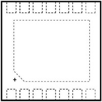
DS4402N+ Maxim Integrated Products, DS4402N+ Datasheet - Page 4

DS4402N+
Manufacturer Part Number
DS4402N+
Description
DAC (D/A Converters) IC DAC 2CH I2C ADJ justable Sink-Source
Manufacturer
Maxim Integrated Products
Datasheet
1.DS4402NTR.pdf
(9 pages)
Specifications of DS4402N+
Resolution
5 bit
Interface Type
Serial (I2C)
Supply Voltage (max)
5.5 V
Supply Voltage (min)
2.7 V
Maximum Operating Temperature
+ 85 C
Mounting Style
SMD/SMT
Minimum Operating Temperature
- 40 C
Number Of Converters
2
Package / Case
TDFN EP
Lead Free Status / RoHS Status
Lead free / RoHS Compliant
Two/Four-Channel, I
Figure 1. Functional Diagram
4
GND
V
DS4404
CC
9, 11
______________________________________________________________________
10
12
14
13
—
—
1
2
3
4
5
6
7
8
SOURCE OR
SINK MODE
V
PIN
CC
4, 5, 12, 14
R
FS0
DS4402
FS0
F8h
9, 11
—
—
10
—
—
13
—
1
2
3
6
7
8
CURRENT
DAC0
A0, A1
NAME
OUT0
OUT1
OUT2
OUT3
OUT0
GND
SDA
SCL
N.C.
FS3
FS2
FS1
FS0
V
EP
CC
SDA SCL A1
SERIAL INTERFACE
I
EACH FOR SINK
2
31-POSITIONS
AND SOURCE
C-COMPATIBLE
MODE
I
I
Ground
Full-Scale Calibration Input. A resistor to ground on these pins determines the full-scale
current for each output. FS0 controls OUT0, FS1 controls OUT1, etc. (DS4402 has only
two inputs: FS0 and FS1.)
Current Output. Sinks or sources the current determined by the I
resistance connected to FSx. (DS4402 has only two outputs: OUT0 and OUT1.)
Address Select Inputs. Tri-level inputs (V
See the Detailed Description section for the nine available device addresses.
Power Supply
No Connection
Exposed Pad. Leave unconnected or connect to GND.
2
2
C Serial Data. Input/output for I
C Serial Clock. Input for I
F9h
A0
FS1
R
FS1
CURRENT
DAC1
2
C Adjustable Current DAC
OUT1
2
C clock.
2
C data.
FS2
R
FS2
FUNCTION
CURRENT
CC
DAC2
, GND, N.C.) determine the I
FAh
OUT2
Pin Description
2
FS3
R
C interface and the
FS3
CURRENT
DAC3
2
DS4404
C slave address.
DS4402/DS4404
OUT3
FBh


