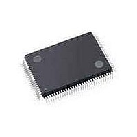
DAC1405D750HW/C1,551 NXP Semiconductors, DAC1405D750HW/C1,551 Datasheet - Page 27

DAC1405D750HW/C1,551
Manufacturer Part Number
DAC1405D750HW/C1,551
Description
DAC (D/A Converters) Dual 14BtDAC 750Msps 4xand 8xnterpolating
Manufacturer
NXP Semiconductors
Datasheet
1.DAC1405D650HWC15.pdf
(45 pages)
Specifications of DAC1405D750HW/C1,551
Number Of Dac Outputs
4
Conversion Rate
650 MSPS
Resolution
14 bit
Supply Voltage (max)
3.6 V
Supply Voltage (min)
3 V
Maximum Operating Temperature
+ 85 C
Mounting Style
SMD/SMT
Maximum Power Dissipation
0.53 W
Minimum Operating Temperature
- 40 C
Supply Current
5 mA
Number Of Converters
2
Settling Time
20 ns
Package / Case
HTQFP-100
Lead Free Status / RoHS Status
Lead free / RoHS Compliant
Other names
935290796551
NXP Semiconductors
DAC1405D650
Product data sheet
10.7.1 NCO in 32-bit
10.7.2 Low-power NCO
10.7.3 Minus 3dB
10.7 Quadrature modulator and Numerically Controlled Oscillator (NCO)
10.8 x / (sin x)
The quadrature modulator allows the 14-bit I and Q data to be mixed with the carrier
signal generated by the NCO.
The frequency of the NCO is programmed over 32-bit and allows the sign of the sine
component to be inverted in order to operate positive or negative, lower or upper single
sideband up-conversion.
When using the NCO, the frequency can be set by the four registers FREQNCO_LSB,
FREQNCO_LISB, FREQNCO_UISB and FREQNCO_MSB over 32 bits.
The frequency for the NCO in 32-bit is calculated as follows:
where M is the decimal representation of FREQ_NCO[31:0].
The phase of the NCO can be set from 0° to 360° by both registers PHINCO_LSB and
PHINCO_MSB over 16 bits.
The default setting is f
When using the low-power NCO, the frequency can be set by the 5 MSB of register
FREQNCO_MSB.
The frequency for the low-power NCO is calculated as follows:
where M is the decimal representation of FREQ_NCO[31:27].
The phase of the low-power NCO can be set by the 5 MSB of the register PHINCO_MSB.
During normal use, a full-scale pattern will also be full scale at the output of the DAC.
Nevertheless, when the I and Q data are simultaneously close to full scale, some clipping
can occur and the Minus_3dB function can be used to reduce the gain by 3 dB in the
modulator. This is to keep a full-scale range at the output of the DAC without added
interferers.
Due to the roll-off effect of the DAC, a selectable FIR filter is inserted to compensate for
the (sin x) / x effect. This filter introduces a DC loss of 3.4 dB. The coefficients are
represented in
f
NCO
f
NCO
=
=
M
--------------
M
--------------
2
×
32
2
×
5
f
Table 34 “Inversion filter
All information provided in this document is subject to legal disclaimers.
s
f
s
Rev. 3 — 10 September 2010
NCO
Dual 14-bit DAC, up to 650 Msps; 2×, 4× and 8× interpolating
= 96 MHz when f
coefficients”.
s
= 640 Msps and the default phase is 0°.
DAC1405D650
© NXP B.V. 2010. All rights reserved.
27 of 45
(1)
(2)


