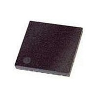
5171N32-U THAT Corporation, 5171N32-U Datasheet - Page 15

5171N32-U
Manufacturer Part Number
5171N32-U
Description
Microphone Preamplifiers High-Perform Digital Pre-Amp Controller
Manufacturer
THAT Corporation
Datasheet
1.5171N32-U.pdf
(20 pages)
Specifications of 5171N32-U
Minimum Operating Temperature
- 40 C
Mounting Style
SMD/SMT
Operating Supply Voltage
3 V to 17 V
Operating Temperature Range
- 40 C to + 85 C
Supply Current
8.3 mA
Supply Voltage (max)
17 V
Supply Voltage (min)
3 V
Thd Plus Noise
0.0003 %
Available Set Gain
13.6 dB to 68.6 dB
Input Offset Voltage
+/- 1.5 mV
Maximum Operating Temperature
+ 85 C
Package / Case
QFN-32
Lead Free Status / RoHS Status
Lead free / RoHS Compliant
THAT5171 High-Performance
Digital Preamplifier Controller IC
Setting the SPI Address Via Hardware Design
application, the address may be set by choosing the
polarity of buffer. During reset, NPN drivers provide
the corresponding GPO with a low logic level ("0"),
while PNP drivers provide a high logic ("1") condition.
The difference in logic levels stems from the base-
emitter junction and associated bias resistors acting
as a pull-up (PNP) or pull-down (NPN) on each pin in
its address-setting mode (during reset).
logic 0. With PNP buffers the immediate post-reset
condition is On. If this is an undesirable condition
the 5171 should be immediately initialized to the
proper state by setting the corresponding GPO out-
put to a logic 1 level.
Flexibility in SPI Address Setting with a Tri-
State Buffer
state buffer. This offers greater flexibility by making
the SPI address independent of the load connected to
the ultimate GPO outputs, shown at GPO'0~GPO'3.
buffer polarity, the tri-state buffer increases the
If a hard-wired SPI address is appropriate for the
After reset, the GPO outputs are initialized to
Figure 11 shows a circuit using a 74LV125A tri-
Besides making the SPI address independent of
5171
RST
A0 - GPO0
A1 - GPO1
A2 - GPO2
A3 - GPO3
15
5171 ADDRESS SHOWN
23
24
25
26
R
47k
0
R
AS 101
B
4k7
Tel: +1 508 478 9200; Fax: +1 508 478 0990; Web: www.thatcorp.com
0
THAT Corporation; 45 Sumner Street; Milford, MA 01757-1656; USA
A
R
47k
1
R
B
4k7
B
Figure 11. 5171 device addressing with buffered GPO outputs.
1
Copyright © 2010, THAT Corporation; All rights reserved.
(=5
A
R
47k
DEC)
2
R
4k7
B
2
A
R
47k
3
B
74LV125A
3.3V
Page 15 of 20
A
B
C
D
E
OE
output drive compared to that available from the
5171. One additional benefit of the circuit shown is
that during reset, the buffers prevent the address-
setting resistors from turning on circuitry connected
to the GPO' connections. During reset, the GPO out-
put buffers, sections A-D, are tri-stated by their out-
put
complementing the /RST line using inverter E.
down resistors R0A through R2B. In the example
above the address is "101b" or "5d". The value of the
pull-up resistors typically range from 4.7k to 47k.
Add R4B to Ensure Future Compatibility
to use GPO3 as an input to set alternate SPI opera-
tion modes. To ensure compatibility with future ver-
sions of the 5171, current designs should include
R3B.
Field Programming the SPI Address
combination of strong pull-up and weak pull-down
may be used in conjunction with switches, links, or
jumpers as shown in Figure 11 in the dotted box. In
the above example the pull-up is 4.7kΩ, the pull-
down is 47kΩ.
GPO’0
GPO’1
GPO’2
GPO’3
The 5171 SPI address is set by pull-up or pull-
In future revisions of the 5171, THAT has plans
If the SPI address must be field programmable, a
enable
R
A0
R
/OE.
J0
47k
4k7
0
0
B
A
FIELD PROGRAMMING
ALTERNATIVE FOR
THE SPI ADDRESS
R
R
A1
4k7
47k
1
J1
1
This
A
B
R
R
A2
J2
4k7
47k
2
2
Document 600133 Rev 04
A
B
is
R
A3
47k
3
ADDRESS
accomplished
(=“5
B
“101
DEC
3.3V
B
”
”)
by


