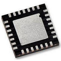
WM8986GECO/V Wolfson Microelectronics, WM8986GECO/V Datasheet - Page 55

WM8986GECO/V
Manufacturer Part Number
WM8986GECO/V
Description
Audio Amplifiers Class D Headphone DAC + Line Out
Manufacturer
Wolfson Microelectronics
Datasheet
1.WM8986GECOV.pdf
(88 pages)
Specifications of WM8986GECO/V
Product
Class-D
Output Power
40 mW
Thd Plus Noise
- 86 dB
Operating Supply Voltage
1.71 V to 3.6 V, 2.5 V to 3.6 V
Maximum Operating Temperature
+ 85 C
Mounting Style
SMD/SMT
Audio Load Resistance
16 Ohms
Minimum Operating Temperature
- 40 C
Output Signal Type
Differential
Supply Voltage (max)
3.6 V
Supply Voltage (min)
1.71 V, 2.5 V
Output Type
Differential
Package / Case
QFN-28
Lead Free Status / RoHS Status
Lead free / RoHS Compliant
Production Data
MASTER CLOCK AND PHASE LOCKED LOOP (PLL)
w
Table 45 Sample Rate Control
The WM8986 has an on-chip phase-locked loop (PLL) circuit that can be used to:
Generate master clocks for the WM8986 audio functions from another external clock, e.g. in
telecoms applications.
Generate and output (on pin CSB/GPIO1) a clock for another part of the system that is derived from
an existing audio master clock.
Figure shows the PLL and internal clocking on the WM8986.
The PLL can be enabled or disabled by the PLLEN register bit.
Table 46 PLLEN Control Bit
Figure 38 PLL and Clock Select Circuit
The PLL frequency ratio R = f
EXAMPLE:
MCLK=12MHz, required clock = 12.288MHz.
R should be chosen to ensure 5 < PLLN < 13. There is a fixed divide by 4 in the PLL and a
R7 (07h)
Additional
Control
R1 (01h)
Power
management 1
REGISTER
ADDRESS
PLLN = int R
PLLK = int (2
3:1
5
24
BIT
(R-PLLN))
SR
2
/f
PLLEN
1
LABEL
(see Figure ) can be set using the register bits PLLK and PLLN:
000
0
DEFAULT
PLL enable
0 = PLL off
1 = PLL on
Approximate sample rate (configures the
coefficients for the internal digital filters):
000 = 48kHz
001 = 32kHz
010 = 24kHz
011 = 16kHz
100 = 12kHz
101 = 8kHz
110-111 = reserved
DESCRIPTION
PD, Rev 4.1, June 2009
WM8986
55


