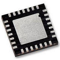
WM8986GECO/V Wolfson Microelectronics, WM8986GECO/V Datasheet - Page 50

WM8986GECO/V
Manufacturer Part Number
WM8986GECO/V
Description
Audio Amplifiers Class D Headphone DAC + Line Out
Manufacturer
Wolfson Microelectronics
Datasheet
1.WM8986GECOV.pdf
(88 pages)
Specifications of WM8986GECO/V
Product
Class-D
Output Power
40 mW
Thd Plus Noise
- 86 dB
Operating Supply Voltage
1.71 V to 3.6 V, 2.5 V to 3.6 V
Maximum Operating Temperature
+ 85 C
Mounting Style
SMD/SMT
Audio Load Resistance
16 Ohms
Minimum Operating Temperature
- 40 C
Output Signal Type
Differential
Supply Voltage (max)
3.6 V
Supply Voltage (min)
1.71 V, 2.5 V
Output Type
Differential
Package / Case
QFN-28
Lead Free Status / RoHS Status
Lead free / RoHS Compliant
WM8986
DIGITAL AUDIO INTERFACES
w
The audio interface has three pins:
The clock signals BCLK, and LRC can be outputs when the WM8986 operates as a master, or inputs
when it is a slave (see Master and Slave Mode Operation, below).
Five different audio data formats are supported:
All of these modes are MSB first. They are described in Audio Data Formats, below. Refer to the
Electrical Characteristic section for timing information.
MASTER AND SLAVE MODE OPERATION
The WM8986 audio interface may be configured as either master or slave. As a master interface
device the WM8986 generates BCLK and LRC and thus controls sequencing of the data transfer on
DACDAT. To set the device to master mode register bit MS should be set high. In slave mode
(MS=0), the WM8986 responds with data to clocks it receives over the digital audio interfaces.
AUDIO DATA FORMATS
In Left Justified mode, the MSB is available on the first rising edge of BCLK following an LRC
transition. The other bits up to the LSB are then transmitted in order. Depending on word length,
BCLK frequency and sample rate, there may be unused BCLK cycles before each LRC transition.
Figure 27 Left Justified Audio Interface (assuming n-bit word length)
In Right Justified mode, the LSB is available on the last rising edge of BCLK before a LRC transition.
All other bits are transmitted before (MSB first). Depending on word length, BCLK frequency and
sample rate, there may be unused BCLK cycles after each LRC transition.
Figure 28 Right Justified Audio Interface (assuming n-bit word length)
•
•
•
•
•
•
•
•
DACDAT: DAC data input
LRC: Data Left/Right alignment clock
BCLK: Bit clock, for synchronisation
Left justified
Right justified
I
DSP mode A
DSP mode B
2
S
PD, Rev 4.1, June 2009
Production Data
50


