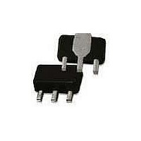
AH125-89PCB1960 TriQuint, AH125-89PCB1960 Datasheet - Page 10

AH125-89PCB1960
Manufacturer Part Number
AH125-89PCB1960
Description
RF Modules & Development Tools .4-2.7GHz Eval Board
Manufacturer
TriQuint
Datasheet
1.AH125-89PCB2140.pdf
(12 pages)
Specifications of AH125-89PCB1960
Board Size
4.25 mm x 4.6 mm x 1.6 mm
Minimum Frequency
400 MHz
Minimum Operating Temperature
- 40 C
Supply Voltage (min)
5 V
Product
RF Modules
Maximum Frequency
3.6 GHz
Supply Voltage (max)
6 V
Supply Current
150 mA
Maximum Operating Temperature
+ 85 C
For Use With/related Products
AH125
Lead Free Status / RoHS Status
Lead free / RoHS Compliant
Other names
1071314
Microstrip line details: width = .031”, spacing = .035”
Circuit Board Material: 0.014” FR4, single layer, 1 oz copper, ε
Application Note
½W High Linearity InGaP HBT Amplifier
Frequency (GHz)
Gain
Input Return Loss
Output Return Loss
EVM
Output P1dB
Output IP3
Pout=+16 dBm/tone, 1MHz spacing
Quiescent Current, Icq
Vcc
TriQuint Semiconductor, Inc • Phone 503-615-9000 • FAX: 503-615-8900 • e-mail: info-sales@tqs.com • Web site: www.TriQuint.com
Pout=+19 dBm
C1
5
4
3
2
1
0
12
Typical Performance at 25°C
802.16-2004 O-FDMA, 64QAM-1/2
1024-FFT, 20 symbols and 30 subchannels
5 MHz Carrier BW
14
R1
EVM vs. Output Power
Output Power (dBm)
16
13.9
1
802.16-2004 O-FDMA, 64QAM-1/2, 1024-FFT, 20 symbols and 30 subchannels, 5 MHz Carrier BW
+28
+49
2.5
9.5
9.4
1.5
U1
2
3
15
14
13
12
10
11
2.5 GHz
2.40
L1
18
14.0
13.1
1.25
+28
+48
150
2.6
8.7
+5
C3
C4
C8
T
2.6 GHz
LEAD
=+25°C
13.7
R2
12.9
+28
+47
2.50
20
2.7
8.2
1.3
2.7 GHz
r
= 4.3,
C2
Gain vs. Frequency
Frequency (GHz)
2.5-2.7 GHz Reference Design
Units
dBm
dBm
mA
dB
dB
dB
22
%
V
2.60
-35
-40
-45
-50
-55
-60
-65
12
Notes:
9.
10. Components shown on the silkscreen but not on the schematic are not used.
11. 0
12. Distance from side edge of C10 to side edge of U1 pin 1 is 55 mils (7.9°@2600 MHz).
13. Distance from end edge of R1 to side edge of U1 pin 1 is 110 mils (15.8°@2600 MHz)..
14. Distance from side edge of C9 to side edge of U1 pin 3 is 90 mils (13.0°@2600 MHz)..
W-CDMA 3GPP Test Model 1+64 DPCH
PAR = 10.2 dB @ 0.01% Probability
3.84 MHz BW
2.70
RF Input
The primary RF microstrip line is 50
T
J1
Ω
LEAD
14
jumpers can be replaced with copper trace in target application.
=+25°C
2.5 GHz
0 Ohms
ACLR vs. Output Power
C1
Output Power (dBm)
2.80
16
2.6 GHz
1pF
R1
-10
-15
-20
-5
0
2.40
Z= 50 Ohm
L=55 mils
18
2.7 GHz
T
LEAD
=+25°C
20
2.50
Return Loss vs. Frequency
C10
0.8pF
Z= 50 Ohm
L=55 mils
Frequency (GHz)
22
Ω
Specifications and information are subject to change without notice
.
2.60
AH125-89PCB2600
55
50
45
40
35
30
1
10
U1
2
2.70
12
3
S11
T
Z= 50 Ohm
L=90 mils
LEAD
OIP3 vs. Output Power/Tone
2.5 GHz
Output Power/Tone (dBm)
=+25°C
S22
14
R4
L1
2.80
VCC
2.6 GHz
16
0 Ohms
C9
0.6pF
18nH
0805CS
0 Ohms
Page 10 of 12 April 2010
R2
18
C3
22pF
2.7 GHz
T
1 MHz tone spacing
LEAD
=+25°C
22pF
R1
20
C4
1000pF
RF Output
J2
22
C8
1uF


