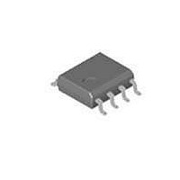
AH322-S8PCB2140 TriQuint, AH322-S8PCB2140 Datasheet - Page 3

AH322-S8PCB2140
Manufacturer Part Number
AH322-S8PCB2140
Description
RF Modules & Development Tools 400-2700MHz Eval Board
Manufacturer
TriQuint
Datasheet
1.AH322-S8PCB2140.pdf
(8 pages)
Specifications of AH322-S8PCB2140
Board Size
6.2 mm x 5 mm x 1.62 mm
Minimum Frequency
400 MHz
Minimum Operating Temperature
- 40 C
Supply Voltage (min)
5 V
Product
RF Modules
Maximum Frequency
2.7 GHz
Output Power
2 W
Supply Voltage (max)
8 V
Supply Current
1400 mA
Maximum Operating Temperature
+ 85 C
For Use With/related Products
AH322
Lead Free Status / RoHS Status
Lead free / RoHS Compliant
Other names
1071299
TriQuint Semiconductor, Inc • Phone 1-800-951-4401 • FAX: 408-577-6633 • e-mail: info-sales@tqs.com • Web site: www.TriQuint.com
AH322
2W High Linearity InGaP HBT Amplifier
Frequency (MHz)
Gain
Input Return Loss
Output Return Loss
Output P1dB
Channel Power
(@-55 dBc IS-95 CDMA ACPR)
Channel Power
(@ -50 dBc WCDMA ACLR)
Output IP3
(21 dBm / tone, 1MHz spacing)
Quiescent Current, Icq
Vpd
Vcc
(4)
-40
-45
-50
-55
-60
-65
-70
Typical RF Performance at 25 ° ° ° ° C
20
19
18
17
16
15
(3)
800
20
IS-95 CDMA, 9 CH. Fwd., ±750 KHz offset frequency, PAR = 9.7 dB @ 0.01 % Prob
(1)
(2)
820
21
824 MHz
Small Signal Performance
ACPR vs. Output Power
Frequency (MHz)
Gain
Output Power (dBm)
840
22
units
dBm
dBm
dBm
dBm
mA
dB
dB
dB
V
V
848 MHz
23
860
S11
+33.0
+24.4
+23.7
+46.2
19.7
824
16
824 - 894 MHz Application Circuit
7
24
880
894 MHz
S22
25
+24.4
+23.7
+46.3
19.7
900
848
+33
600
+5
+5
16
8
0
-5
-10
-15
-20
-25
26
.
+32.6
+23.8
+45.1
19.7
894
+23
13
12
Notes:
1. ACPR test set-up: IS-95 CDMA, 9 channels fwd, ±750 KHz offset, 30 KHz, Meas BW, PAR = 9.7 dB
2. ACLR test set-up: 3GPP WCDMA, TM1±64 DPCH, ±5MHz offset no clipping, PAR = 10.34 dB @
3. OIP3 is measured at 21 dBm / tone output power with 1 MHz spacing.
4. Vpd is used as device power down voltage (low = RF off
5. The edge of L2 is placed at 265 mils from edge of AH322 RFout pin (12 º @ 850 MHz).
6. The edge of C2 is placed at 250 mils from edge of AH322 RFout pin (11 º @ 850 MHz).
7. The edge of C8 is placed at 25 mils from edge of AH322 RFout pin (1 º @ 850 MHz).
8. Do not exceed +5.5V supply or TVS diode D3 will be damaged.
9. Zero ohm jumpers may be replaced with copper traces in the target application layout.
10. DNP implies Do Not Place.
@ 0.01% Prob.
0.01% Probability.
50
47
44
41
38
35
-30
-35
-40
-45
-50
-55
-60
18
20
3GPP WCDMA, TM1+64DPCH, ±5MHz offset Freq., PAR = 10.34 % @ Prob.
19
824 MHz
824 MHz
21
20
OIP3 vs. Output Power
ACLR vs. Output Power
Output Power / tone (dBm)
Output Power (dBm)
22
21
1MHz spacing, 25C
848 MHz
848 MHz
22
).
23
23
894 MHz
894 MHz
24
24
25
25
26
26
April 2009
.


