OM11049,598 NXP Semiconductors, OM11049,598 Datasheet - Page 63
OM11049,598
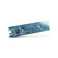
Manufacturer Part Number
OM11049,598
Description
MCU, MPU & DSP Development Tools LPC1114 Demo Boards Cortex M0
Manufacturer
NXP Semiconductors
Datasheet
1.OM11049598.pdf
(66 pages)
Specifications of OM11049,598
Processor To Be Evaluated
LPC1114
Processor Series
LPC11xx
Interface Type
I2C, SPI
Maximum Operating Temperature
+ 85 C
Minimum Operating Temperature
- 40 C
Operating Supply Voltage
3.3 V
Tool Type
Demonstration Board
Core Architecture
ARM
Cpu Core
ARM Cortex M0
Data Bus Width
32 bit
Lead Free Status / RoHS Status
Lead free / RoHS Compliant


NXP Semiconductors
14. Revision history
Table 23.
LPC1111_12_13_14
Product data sheet
Document ID
LPC1111_12_13_14 v.4
Modifications:
LPC1111_12_13_14 v.3
Modifications:
LPC1111_12_13_14 v.2
Modifications:
LPC1111_12_13_14 v.1
Revision history
Release date
20110210
20101110
20100818
20100416
•
•
•
•
•
•
•
•
•
•
•
•
•
•
•
•
•
•
•
•
•
Power consumption graphs added for parts LPC111x/102/202/302
Figure
Parameter V
Typical value for parameter N
I
(minimum) for 2.0 V ≤ V
Section 11.6 “ElectroMagnetic Compatibility (EMC)”
Power-up characterization added
Parts LPC111x/102/202/302 added (LPC1100L series).
Power consumption data for parts LPC111x/102/202/302 added in Table 7.
PLL output frequency limited to 100 MHz in Section 7.15.2.
Description of RESET and WAKEUP functions updated in Section 6.
WDT description updated in Section 7.14. The WDT is a 24-bit timer.
Power profiles added to Section 2 and Section 7 for parts LPC111x/102/202/302.
V
t
Deep-sleep mode functionality changed to allow BOD and watchdog oscillator as the
only analog blocks allowed to remain running in Deep-sleep mode (Section 7.15.5.3).
V
Reset state of pins and start logic functionality added in Table 3 to Table 5.
Section 7.16.1 added.
Section “Memory mapping control” removed.
V
Section 9.4 added.
2
DS
ESD
DD
OH
C-bus pins configured as standard mode pins, parameter I
updated for SPI in master mode (Table 17).
range changed to 3.0 V ≤ V
and I
All information provided in this document is subject to legal disclaimers.
limit changed to −6500 V (min) /+6500 V (max) in Table 6.
17).
OH
Rev. 4 — 10 February 2011
hys
specifications updated for high-drive pins in Table 7.
Data sheet status
Product data sheet
Product data sheet
Product data sheet
Product data sheet
for I
2
C bus pins: typical value corrected V
DD
≤ 3.6 V.
endu
DD
(Section 10.1 “Power-up ramp
added in
≤ 3.6 V in Table 15.
-
-
-
Change notice
-
32-bit ARM Cortex-M0 microcontroller
Table 12 “Flash
LPC1111/12/13/14
added.
Supersedes
LPC1111_12_13_14 v.3
LPC1111_12_13_14 v.2
LPC1111_12_13_14 v.1
-
hys
characteristics”.
OL
= 0.05V
changed to 3.5 mA
conditions”).
© NXP B.V. 2011. All rights reserved.
(Figure 13
DD
in
Table
to
63 of 66
7.
Related parts for OM11049,598
Image
Part Number
Description
Manufacturer
Datasheet
Request
R

Part Number:
Description:
NXP Semiconductors designed the LPC2420/2460 microcontroller around a 16-bit/32-bitARM7TDMI-S CPU core with real-time debug interfaces that include both JTAG andembedded trace
Manufacturer:
NXP Semiconductors
Datasheet:

Part Number:
Description:
NXP Semiconductors designed the LPC2458 microcontroller around a 16-bit/32-bitARM7TDMI-S CPU core with real-time debug interfaces that include both JTAG andembedded trace
Manufacturer:
NXP Semiconductors
Datasheet:
Part Number:
Description:
NXP Semiconductors designed the LPC2468 microcontroller around a 16-bit/32-bitARM7TDMI-S CPU core with real-time debug interfaces that include both JTAG andembedded trace
Manufacturer:
NXP Semiconductors
Datasheet:
Part Number:
Description:
NXP Semiconductors designed the LPC2470 microcontroller, powered by theARM7TDMI-S core, to be a highly integrated microcontroller for a wide range ofapplications that require advanced communications and high quality graphic displays
Manufacturer:
NXP Semiconductors
Datasheet:
Part Number:
Description:
NXP Semiconductors designed the LPC2478 microcontroller, powered by theARM7TDMI-S core, to be a highly integrated microcontroller for a wide range ofapplications that require advanced communications and high quality graphic displays
Manufacturer:
NXP Semiconductors
Datasheet:
Part Number:
Description:
The Philips Semiconductors XA (eXtended Architecture) family of 16-bit single-chip microcontrollers is powerful enough to easily handle the requirements of high performance embedded applications, yet inexpensive enough to compete in the market for hi
Manufacturer:
NXP Semiconductors
Datasheet:
Part Number:
Description:
The XA-S3 device is a member of Philips Semiconductors? XA(eXtended Architecture) family of high performance 16-bitsingle-chip microcontrollers
Manufacturer:
NXP Semiconductors
Datasheet:

Part Number:
Description:
The NXP BlueStreak LH75401/LH75411 family consists of two low-cost 16/32-bit System-on-Chip (SoC) devices
Manufacturer:
NXP Semiconductors
Datasheet:
Part Number:
Description:
The NXP LPC3130/3131 combine an 180 MHz ARM926EJ-S CPU core, high-speed USB2
Manufacturer:
NXP Semiconductors
Datasheet:
Part Number:
Description:
The NXP LPC3141 combine a 270 MHz ARM926EJ-S CPU core, High-speed USB 2
Manufacturer:
NXP Semiconductors
Part Number:
Description:
The NXP LPC3143 combine a 270 MHz ARM926EJ-S CPU core, High-speed USB 2
Manufacturer:
NXP Semiconductors

Part Number:
Description:
The NXP LPC3152 combines an 180 MHz ARM926EJ-S CPU core, High-speed USB 2
Manufacturer:
NXP Semiconductors
Part Number:
Description:
The NXP LPC3154 combines an 180 MHz ARM926EJ-S CPU core, High-speed USB 2
Manufacturer:
NXP Semiconductors

Part Number:
Description:
Standard level N-channel enhancement mode Field-Effect Transistor (FET) in a plastic package using NXP High-Performance Automotive (HPA) TrenchMOS technology
Manufacturer:
NXP Semiconductors
Datasheet: