LFXP2-5E-B-EVN Lattice, LFXP2-5E-B-EVN Datasheet - Page 16
LFXP2-5E-B-EVN
Manufacturer Part Number
LFXP2-5E-B-EVN
Description
MCU, MPU & DSP Development Tools LatticeXP2 Brevia Dev kit
Manufacturer
Lattice
Series
-r
Type
FPGAr
Datasheets
1.LFXP2-5E-B-EVN.pdf
(25 pages)
2.LFXP2-5E-B-EVN.pdf
(4 pages)
3.LFXP2-5E-B-EVN.pdf
(4 pages)
Specifications of LFXP2-5E-B-EVN
Processor To Be Evaluated
LFXP2-5E-6TN144C
Data Bus Width
8 bit
Interface Type
RS-232, JTAG, SPI
Operating Supply Voltage
3.3 V
Silicon Manufacturer
Lattice Semiconductor
Silicon Family Name
LatticeXP2
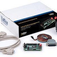
Kit Contents
Evaluation Board, USB Cables, AC Adapter, Quick Start Guide
Features
Serial RS232 Interface, JTAG Interface
Svhc
No
Rohs Compliant
Yes
Contents
Board, Cables, Documentation, Power Supply
Lead Free Status / RoHS Status
Lead free / RoHS Compliant
For Use With/related Products
LFXP2-5E-6TN144C
Available stocks
Company
Part Number
Manufacturer
Quantity
Price
Company:

Part Number:
LFXP2-5E-B-EVN
Manufacturer:
Lattice
Quantity:
8


Lattice Semiconductor
SRAM Interface
The LatticeXP2 Brevia Evaluation Board provides 1Mbit of asynchronous SRAM memory in a 128K x 8-bit configu-
ration.
Table 7.
Configuration Interface
Jumper 5 controls the XP2 CFG0 input control pin.
Table 8. Configuration Interface
The factory default setting on J5 is to leave it unshunted. CFG0 has a weak pullup resistor.
SRAM Interface
FPGA SRAM 1 Mbit (U2)
SRAM Signal Name
SRAM_Web
SRAM_CSb
SRAM_Oeb
Addr_10
Addr_11
Addr_12
Addr_13
Addr_14
Addr_15
Addr_16
Data_0
Data_1
Data_2
Data_3
Data_4
Data_5
Data_6
Data_7
Addr_0
Addr_1
Addr_2
Addr_3
Addr_4
Addr_5
Addr_6
Addr_7
Addr_8
Addr_9
CFG0
1
0
16
FPGA Pin
Position
Number
Jumper
119
120
121
122
123
124
125
127
129
130
131
132
133
134
137
138
141
142
143
144
1-2
2-3
10
1
2
5
6
7
8
9
LatticeXP2 Brevia Development Kit
User’s Guide
Related parts for LFXP2-5E-B-EVN
Image
Part Number
Description
Manufacturer
Datasheet
Request
R

Part Number:
Description:
FPGA - Field Programmable Gate Array 5K LUTs 146I/O Inst- on DSP 1.2V -5 Spd
Manufacturer:
Lattice
Datasheet:

Part Number:
Description:
Programmable Logic IC Development Tools Lattice XP2 Brevia Dev Kit
Manufacturer:
Lattice
Datasheet:

Part Number:
Description:
FPGA - Field Programmable Gate Array 5K LUTs 172 I/O Inst on DSP 1.2V -5 Spd
Manufacturer:
Lattice
Datasheet:
Part Number:
Description:
FPGA - Field Programmable Gate Array 5K LUTs 100 I/O Inst on DSP 1.2V -5 Spd
Manufacturer:
Lattice
Datasheet:

Part Number:
Description:
FPGA - Field Programmable Gate Array 5K LUTs 172I/O Inst- on DSP 1.2V -5 Spd
Manufacturer:
Lattice
Datasheet:

Part Number:
Description:
FPGA - Field Programmable Gate Array 5K LUTs 100I/O Inst- on DSP 1.2V -5 Spd
Manufacturer:
Lattice
Datasheet:

Part Number:
Description:
FPGA LatticeXP2 Family 5000 Cells Flash Technology 1.2V 256-Pin FTBGA
Manufacturer:
LATTICE SEMICONDUCTOR
Datasheet:
Part Number:
Description:
FPGA LatticeXP2 Family 5000 Cells Flash Technology 1.2V 256-Pin FTBGA
Manufacturer:
LATTICE SEMICONDUCTOR
Datasheet:
Part Number:
Description:
IC DSP 5KLUTS 100I/O 144TQFP
Manufacturer:
Lattice
Datasheet:
Part Number:
Description:
IC DSP 5KLUTS 86I/O 132CSBGA
Manufacturer:
Lattice
Datasheet:
Part Number:
Description:
IC DSP 5KLUTS 86I/O 132CSBGA
Manufacturer:
Lattice
Datasheet:
Part Number:
Description:
IC DSP 5KLUTS 146I/O 208PQFP
Manufacturer:
Lattice
Datasheet:
Part Number:
Description:
IC DSP 5KLUTS 146I/O 208PQFP
Manufacturer:
Lattice
Datasheet:
Part Number:
Description:
IC DSP 5KLUTS 172I/O 256FTBGA
Manufacturer:
Lattice
Datasheet:
Part Number:
Description:
IC FPGA 5KLUTS 86I/O 132-BGA
Manufacturer:
Lattice
Datasheet: