NCP3125AGEVB ON Semiconductor, NCP3125AGEVB Datasheet - Page 15
NCP3125AGEVB
Manufacturer Part Number
NCP3125AGEVB
Description
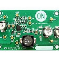
Power Management Modules & Development Tools NCP3125 Evaluation Board
Manufacturer
ON Semiconductor
Type
DC/DC Switching Converters, Regulators & Controllersr
Datasheets
1.NCP3125AGEVB.pdf
(22 pages)
2.NCP3125AGEVB.pdf
(1 pages)
3.NCP3125AGEVB.pdf
(4 pages)
4.NCP3125AGEVB.pdf
(1 pages)
Specifications of NCP3125AGEVB
Maximum Operating Temperature
+ 125 C
Minimum Operating Temperature
- 40 C
Operating Supply Voltage
4.5 V to 13.2 V
Product
Power Management Modules
For Use With/related Products
NCP3125
Lead Free Status / RoHS Status
Lead free / RoHS Compliant


R
R
V
V
associated standard R
Table 5. OUTPUT VOLTAGE SETTINGS
1
2
OUT
REF
The most frequently used output voltages and their
V
O
0.8
1.2
1.5
1.8
2.5
3.3
5.0
(V)
R
2
= Top resistor divider
= Bottom resistor divider
= Output voltage
= Regulator reference voltage
+ R
1
1
and R
@
R
1
4.99
12.7
21.5
31.6
52.3
1.0
V
10
(kW)
2
OUT
values are listed in Table 5.
V
REF
* V
REF
R
Open
2
11.5
10.2
10
10
10
10
(kW)
(eq. 39)
http://onsemi.com
15
Transconductance Error Amplifier can be calculated using
the method described below. The method serves to provide
a good starting place for compensation of a power supply.
The values can be adjusted in real time using the
compensation tool comp calc, available for download at
ON Semiconductor’s website.
least 2X the value of R
noise. Using the 2X assumption, R
the feed through capacitor can be calculated as shown
below:
The compensation components for the Pseudo Type III
The value of the feed through resistor should always be at
2
to minimize error from feed through
F
will be set to 20 kW and
Related parts for NCP3125AGEVB
Image
Part Number
Description
Manufacturer
Datasheet
Request
R

Part Number:
Description:
4 A Synchronous PWM Switching Converter
Manufacturer:
ON Semiconductor
Datasheet:
Part Number:
Description:
BOARD EVALUATION NCP3125 CERAMIC
Manufacturer:
ON Semiconductor
Datasheet:
Part Number:
Description:
ON Semiconductor [VOLTAGE REGULATOR]
Manufacturer:
ON Semiconductor
Datasheet:
Part Number:
Description:
357-036-542-201 CARDEDGE 36POS DL .156 BLK LOPRO
Manufacturer:
ON Semiconductor
Datasheet:
Part Number:
Description:
357-036-542-201 CARDEDGE 36POS DL .156 BLK LOPRO
Manufacturer:
ON Semiconductor
Datasheet:
Part Number:
Description:
357-036-542-201 CARDEDGE 36POS DL .156 BLK LOPRO
Manufacturer:
ON Semiconductor
Datasheet:
Part Number:
Description:
357-036-542-201 CARDEDGE 36POS DL .156 BLK LOPRO
Manufacturer:
ON Semiconductor
Datasheet:
Part Number:
Description:
357-036-542-201 CARDEDGE 36POS DL .156 BLK LOPRO
Manufacturer:
ON Semiconductor
Datasheet:
Part Number:
Description:
357-036-542-201 CARDEDGE 36POS DL .156 BLK LOPRO
Manufacturer:
ON Semiconductor
Datasheet:
Part Number:
Description:
357-036-542-201 CARDEDGE 36POS DL .156 BLK LOPRO
Manufacturer:
ON Semiconductor
Datasheet:
Part Number:
Description:
357-036-542-201 CARDEDGE 36POS DL .156 BLK LOPRO
Manufacturer:
ON Semiconductor
Datasheet:
Part Number:
Description:
357-036-542-201 CARDEDGE 36POS DL .156 BLK LOPRO
Manufacturer:
ON Semiconductor
Datasheet:
Part Number:
Description:
357-036-542-201 CARDEDGE 36POS DL .156 BLK LOPRO
Manufacturer:
ON Semiconductor
Datasheet:
Part Number:
Description:
Manufacturer:
ON Semiconductor
Datasheet: