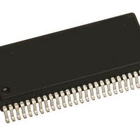
KIT33937AEKEVBE Freescale Semiconductor, KIT33937AEKEVBE Datasheet - Page 31

KIT33937AEKEVBE
Manufacturer Part Number
KIT33937AEKEVBE
Description
Power Management Modules & Development Tools 3-PHASE FET PRE-DRIV
Manufacturer
Freescale Semiconductor
Type
MOSFET & Power Driverr
Datasheet
1.MCZ33937AEKR2.pdf
(48 pages)
Specifications of KIT33937AEKEVBE
Interface Type
SPI
Product
Power Management Modules
Silicon Manufacturer
Freescale
Silicon Core Number
MC33937
Kit Application Type
Power Management
Application Sub Type
FET Driver
Kit Contents
Board, CD
Rohs Compliant
Yes
For Use With/related Products
MC33937
the appropriate mask bit is set. The INT will be held in the
High state until the fault is removed, and the appropriate bit
in the Status Register 0 is cleared by the CLINT1 command.
This fault reporting mechanism is described in detail in the
Logic Commands and Registers
HOLD OFF CIRCUIT
absence of V
small current source, generated from VSUP, typically
100 µA, is mirrored and pulls all the output gate drive pins low
when V
when VLS is lower than the VLS_Disable threshold. A
minimum of approximately 3.0 V is required on VSUP to
energize the Hold off circuit.
CHARGE PUMP
elements required to implement a charge pump, when
combined with external capacitors and diodes for enhanced
low voltage operation.
using the charge pump (see
Analog Integrated Circuit Device Data
Freescale Semiconductor
The IC guarantees the output FETs are turned off in the
The Charge Pump circuit provides the basic switching
When the 33937 is connected per the typical application
DD
is less than about 3.0 V,
DD
or V
PWR
by means of the Hold off circuit. A
Figure
section.
RST
22), the regulation path
is active (low), or
for VLS includes the charge pump and a linear regulator. The
regulation set point for the linear regulator is nominally at
15.34 V. As long as VLS output voltage (VLS
than the VLS analog regulator threshold (VLS
V
until VLS
with this cycle even when there is overlap in the thresholds,
due to the design of the regulator system.
dependent on the pump capacitor value and quality, the
pump frequency (nominally 130 kHz), and the Rdson of the
pump FETs. The effective charge voltage for the pump
capacitor would be V
transfer would then be C
Multiplying by the switch frequency gives the theoretical
current the pump can transfer: F
2*V
charge pump (Trickle Charge Pump - see
used to maintain the High Side drivers’ gate V
percent duty cycle modes.
THREG
If VLS
V
The maximum current the charge pump can supply is
NOTE: There is also another smaller, fully integrated
DIODE
HYST
, the charge pump is not active.
OUT
OUT
).
is approximately 200 mV. VLS
< VLS
> VLS
FUNCTIONAL INTERNAL BLOCK DESCRIPTION
ATH
ATH
SYS
– V
– V
PUMP
– 2 * V
THREG
THREG
* (V
DIODE
PUMP
the charge pump turns ON
+ V
SYS
HYST
. The total charge
* C
– 2*V
ATH
PUMP
Figure
will not interfere
DIODE
OUT
ATH
GS
* (V
2), which is
) is greater
in 100
) minus
).
SYS
–
33937
31


