K3012P Vishay, K3012P Datasheet - Page 2
K3012P
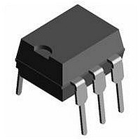
Manufacturer Part Number
K3012P
Description
Triac & SCR Output Optocouplers Phototriac Output
Manufacturer
Vishay
Specifications of K3012P
Isolation Voltage
3750 Vrms
Configuration
1
Maximum Continuous Output Current
100 mA
Maximum Input Current
80 mA
Maximum Operating Temperature
+ 85 C
Maximum Power Dissipation
350 mW
Maximum Reverse Diode Voltage
5 V
Minimum Operating Temperature
- 40 C
Mounting Style
Through Hole
Output Type
AC
Package / Case
DIL
Typical Input Voltage
1.25 V
Zero-crossing Circuit
No
Output Device
Triac
Peak Output Voltage (vdrm)
250 V
Maximum Input Voltage
1.6 V
Maximum Output Voltage
175 VAC
Minimum Trigger Current
2 mA (Typ)
No. Of Channels
1
Optocoupler Output Type
Phototriac
Input Current
50mA
Output Voltage
250V
Opto Case Style
DIP
No. Of Pins
6
Mounting Type
Through Hole
Approval Bodies
UL, VDE
Blocking Voltage
250V
Rohs Compliant
Yes
Lead Free Status / RoHS Status
Lead free / RoHS Compliant
Lead Free Status / RoHS Status
Lead free / RoHS Compliant, Lead free / RoHS Compliant
Available stocks
Company
Part Number
Manufacturer
Quantity
Price


K3010P, K3010PG Series
Vishay Semiconductors
Notes
(1)
(2)
Notes
(1)
(2)
(3)
www.vishay.com
520
ABSOLUTE MAXIMUM RATINGS
PARAMETER
INPUT
Reverse voltage
Forward current
Forward surge current
Power dissipation
Junction temperature
OUTPUT
Off state output terminal voltage
On state RMS current
Peak surge current, non-repetitive
Power dissipation
Junction temperature
COUPLER
Isolation test voltage (RMS)
Total power dissipation
Ambient temperature range
Storage temperature range
Soldering temperature
ELECTRICAL CHARACTERISTICS
PARAMETER
INPUT
Forward voltage
Junction capacitance
OUTPUT
Forward peak off-state voltage
(repetitive)
Peak on-state voltage
Critical rate of rise of off-state voltage
Collector emitter saturation voltage
Holding current
Stresses in excess of the absolute maximum ratings can cause permanent damage to the device. Functional operation of the device is not
implied at these or any other conditions in excess of those given in the operational sections of this document. Exposure to absolute
maximum ratings for extended periods of the time can adversely affect reliability.
Refer to wave profile for soldering conditions for through hole devices (DIP).
Minimum and maximum values are testing requirements. Typical values are characteristics of the device and are the result of engineering
evaluation. Typical values are for information only and are not part of the testing requirements.
Test voltage must be applied within dV/dt ratings.
I
FT
is defined as a minimum trigger current.
(2)
For technical questions, contact:
Optocoupler, Phototriac Output, 250 V
V
I
I
TEST CONDITION
F
2 mm from case, t ≤ 10 s
FT
S
V
= 10 mA, V
R
= 3 V, R
I
I
RDM
= 0, I
TEST CONDITION
(1)
TM
= 0, f = 1 MHz
I
(1)
F
= 50 mA
= 100 mA
(T
= 100 nA
t
t
FT
p
P
(T
amb
t = 1 s
≤ 10 ms
≤ 10 μs
L
= 30 mA
amb
= 150 Ω
S
= 25 °C, unless otherwise specified)
≥ 3 V
= 25 °C, unless otherwise specified)
COUPLER
optocoupleranswers@vishay.com
K3010PG
K3011PG
K3012PG
K3010P
K3011P
K3012P
PART
(3)
SYMBOL
V
T
P
P
I
I
I
V
T
P
T
FSM
TRM
TMS
V
DRM
amb
diss
T
diss
T
I
ISO
stg
sld
tot
F
R
j
j
SYMBOL
dV/d
V
dV/d
DRM
V
I
I
I
I
I
I
V
C
I
FT
FT
FT
FT
FT
FT
TM
H
F
j
tcrq
tcr
(2)
- 55 to + 100
DRM
- 40 to + 85
MIN.
250
0.1
VALUE
5300
100
100
250
100
300
100
350
260
1.5
80
5
3
TYP.
1.25
100
1.5
0.2
50
10
8
8
5
5
2
2
Document Number: 83504
Rev. 2.0, 05-Mar-10
MAX.
1.6
15
15
10
10
3
5
5
UNIT
V
mW
mW
mW
mA
mA
°C
°C
RMS
°C
°C
°C
V
A
V
A
UNIT
mA
mA
mA
mA
mA
mA
pF
nA
nA
μA
V
V
V
Related parts for K3012P
Image
Part Number
Description
Manufacturer
Datasheet
Request
R

Part Number:
Description:
Optocoupler with Phototriac Output
Manufacturer:
Vishay Telefunken
Datasheet:

Part Number:
Description:
357-036-542-201 CARDEDGE 36POS DL .156 BLK LOPRO
Manufacturer:
Vishay
Datasheet:
Part Number:
Description:
357-036-542-201 CARDEDGE 36POS DL .156 BLK LOPRO
Manufacturer:
Vishay
Datasheet:
Part Number:
Description:
357-036-542-201 CARDEDGE 36POS DL .156 BLK LOPRO
Manufacturer:
Vishay
Datasheet:
Part Number:
Description:
357-036-542-201 CARDEDGE 36POS DL .156 BLK LOPRO
Manufacturer:
Vishay
Datasheet:
Part Number:
Description:
357-036-542-201 CARDEDGE 36POS DL .156 BLK LOPRO
Manufacturer:
Vishay
Datasheet:
Part Number:
Description:
357-036-542-201 CARDEDGE 36POS DL .156 BLK LOPRO
Manufacturer:
Vishay
Datasheet:
Part Number:
Description:
357-036-542-201 CARDEDGE 36POS DL .156 BLK LOPRO
Manufacturer:
Vishay
Datasheet:
Part Number:
Description:
357-036-542-201 CARDEDGE 36POS DL .156 BLK LOPRO
Manufacturer:
Vishay
Datasheet:
Part Number:
Description:
357-036-542-201 CARDEDGE 36POS DL .156 BLK LOPRO
Manufacturer:
Vishay
Datasheet:
Part Number:
Description:
357-036-542-201 CARDEDGE 36POS DL .156 BLK LOPRO
Manufacturer:
Vishay
Datasheet:
Part Number:
Description:
357-036-542-201 CARDEDGE 36POS DL .156 BLK LOPRO
Manufacturer:
Vishay
Datasheet:
Part Number:
Description:
357-036-542-201 CARDEDGE 36POS DL .156 BLK LOPRO
Manufacturer:
Vishay
Datasheet:
Part Number:
Description:
357-036-542-201 CARDEDGE 36POS DL .156 BLK LOPRO
Manufacturer:
Vishay
Datasheet:
Part Number:
Description:
357-036-542-201 CARDEDGE 36POS DL .156 BLK LOPRO
Manufacturer:
Vishay
Datasheet: