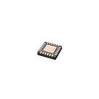
TFA9879HN/N1,157 NXP Semiconductors, TFA9879HN/N1,157 Datasheet - Page 34

TFA9879HN/N1,157
Manufacturer Part Number
TFA9879HN/N1,157
Description
IC AMP AUDIO DGTL MONO D 24HVQFN
Manufacturer
NXP Semiconductors
Type
Class Dr
Datasheet
1.TFA9879HNN1118.pdf
(60 pages)
Specifications of TFA9879HN/N1,157
Output Type
1-Channel (Mono)
Package / Case
24-VFQFN Exposed Pad
Max Output Power X Channels @ Load
2.75W x 1 @ 4 Ohm
Voltage - Supply
2.5 V ~ 5.5 V
Features
Depop, Digital Inputs, I²C, I²S, Mute, Short-Circuit and Thermal Protection, Tone and Volume Control
Mounting Type
Surface Mount
Product
Class-D
Output Power
2.75 W
Thd Plus Noise
0.02 %
Operating Supply Voltage
3.7 V
Supply Current
5.7 mA
Mounting Style
SMD/SMT
Audio - Load Impedance
4 Ohms, 8 Ohms
Audio Load Resistance
4 Ohms, 8 Ohms
Input Signal Type
Serial
Supply Voltage (max)
5.5 V
Supply Voltage (min)
2.5 V
Lead Free Status / RoHS Status
Lead free / RoHS Compliant
NXP Semiconductors
TFA9879
Product data sheet
10.4.10 Miscellaneous status
Table 33.
Bit
15
14
13
12:11 reserved
10:9
8
7
6
5
4
PORA
IBP(2)
OFP(2)
UFP(2)
IBP(1)
OFP(1)
Symbol
reserved
PS
AMP
Miscellaneous status register (address 15h) bit description
All information provided in this document is subject to legal disclaimers.
Access
R
R
R
R
R
R
R
R
Rev. 02 — 15 October 2010
invalid bit clock protection on serial interface input 2:
underfrequency protection on serial interface input 2:
invalid bit clock protection on serial interface input 1:
Description
power stage status:
analog 1V8 regulator status:
Amplifier mode status:
overfrequency protection on serial interface input 2:
overfrequency protection on serial interface input 1:
0: class-D audio amplifier power stage floating
1: class-D audio amplifier power stage switching; PWM signals
on pins OUTA and OUTB
0: 1V8 analog regulator is off or output voltage level is too low
1: 1V8 analog regulator output is available and correct
00: amplifier is off
01: startup
10: startup
11: amplifier is functional
0: the ratio in frequency between the signal on pin SCK2 and
the signal on pin LRCK2 is valid for the selected interface
format
1: the ratio in frequency between the signal on pin SCK2 and
the signal on pin LRCK2 is invalid for the selected interface
format
0: the frequency of the signal on pin LRCK2 is in line with (or
lower than) the selected interface format
1: the frequency of the signal on pin LRCK2 is higher than the
selected interface format
0: the frequency of the signal on pin LRCK2 is in line with (or
higher than) the selected interface format
1: the frequency of the signal on pin LRCK2 is lower than the
selected interface format
0: the ratio in frequency between the signal on pin SCK1 and
the signal on pin LRCK1 is valid for the selected interface
format
1: the ratio in frequency between the signal on pin SCK1 and
the signal on pin LRCK1 is invalid for the selected interface
format
0: the frequency of the signal on pin LRCK1 is in line with (or
lower than) the selected interface format
1: the frequency of the signal on pin LRCK1 is higher than the
selected interface format
Mono BTL class-D audio amplifier with digital input
TFA9879
© NXP B.V. 2010. All rights reserved.
34 of 60


