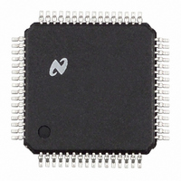
CLC030VEC National Semiconductor, CLC030VEC Datasheet - Page 14

CLC030VEC
Manufacturer Part Number
CLC030VEC
Description
IC SERIALIZER VIDEO DGTL 64-TQFP
Manufacturer
National Semiconductor
Datasheet
1.CLC030VEC.pdf
(29 pages)
Specifications of CLC030VEC
Function
Serializer
Data Rate
1.485Gbps
Input Type
CMOS
Output Type
CMOS
Number Of Inputs
7
Number Of Outputs
7
Voltage - Supply
2.5V, 3.3V
Operating Temperature
0°C ~ 70°C
Mounting Type
Surface Mount
Package / Case
64-TQFP
Lead Free Status / RoHS Status
Contains lead / RoHS non-compliant
Other names
*CLC030VEC
Available stocks
Company
Part Number
Manufacturer
Quantity
Price
Company:
Part Number:
CLC030VEC
Manufacturer:
NSC
Quantity:
5 510
Company:
Part Number:
CLC030VEC
Manufacturer:
TI
Quantity:
5 510
www.national.com
Device Operation
logic-0. The TPG or BIST is halted by resetting TPG Enable.
The serial output data is present at the SDO outputs during
TPG or BIST operation.
Caution ! When attempting to use the TPG or BIST imme-
diately after applying power or resetting the device, the TPG
defaults to the 270Mbps SD rate and expects a V
frequency of 27MHz as input. This is because the code for
the test pattern in the TEST 0 register is set to 00h (525 line,
30 frame, 27MHz, NTSC 4x3 reference black). Attempting to
apply a V
according to the setting in the TEST 0 register, may result in
the PLL locking up while attempting to slew to its maximum
possible frequency. This situation is not recoverable by the
use of the device RESET input. To recover from this condi-
tion, power must be removed and re-applied to the device.
Proper conditioning of the V
an internal pull down device, is mandatory to prevent admis-
sion of noise or unwanted signals at any time, especially
during power-up or reset sequences. It is strongly recom-
mended that V
and configuration is completed.
Example: Enable the TPG Mode to use the NTSC 270Mbps
color bars as the BIST and TPG pattern. Enable TPG opera-
tion using the I/O port.
CLK
frequency higher than the device expects,
CLK
not be applied until device initialization
CLK
(Continued)
input, which does not have
CLK
clock
14
1. Set ANC/CTRL to a logic-low.
2. Set RD/WR to a logic-low.
3. Present 00Dh to AD[9:0] as the TEST 0 register ad-
4. Toggle ACLK.
5. Present 303h to AD[9:0] as the register data (525 line,
6. Toggle ACLK.
7. Set TPG ENABLE (I/O Port, bit 7) to a logic-high.
8. Toggle ACLK.
9. The PASS/FAIL indicator (I/O Port, bit 6) is monitored
CONFIGURATION AND CONTROL REGISTERS
The configuration and control registers store data which
configures the operational modes of the CLC030 or which
result from its operation. Many of these registers can be
mapped to the multi-function I/O bus to make them available
as external I/O functions. These functions and initial values
are summarized in Table 1 and detailed in Table 2. The
power-on default condition for the multi-function I/O port is
indicated in Table 1 and detailed in Table 6.
dress.
30 frame, 27MHz, NTSC 4x3, color bars (SMPTE
125M)).
for the result of the test. Alternatively, the TEST 0 regis-
ter may be read. Bit 7 is the Pass/Fail indicator bit.


