CLC030VEC National Semiconductor, CLC030VEC Datasheet
CLC030VEC
Specifications of CLC030VEC
Available stocks


Related parts for CLC030VEC


CLC030VEC Summary of contents
Page 1
... Separate power pins for the output driver, PLL and the serializer improve power supply rejection, output jitter and noise performance. Order Number CLC030VEC © 2006 National Semiconductor Corporation The CLC030’s internal circuitry is powered from +2.5V and the I/O circuitry from a +3.3V supply. Power dissipation is typically 430mW at 1.485Gbps including two 75Ω ...
Page 2
Typical Application www.national.com 2 20000301 ...
Page 3
Block Diagram 3 20000302 www.national.com ...
Page 4
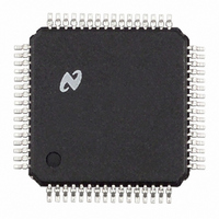
... Connection Diagram www.national.com 64-Pin TQFP Order Number CLC030VEC See NS Package Number VEC-64A 4 20000303 ...
Page 5
Absolute Maximum Ratings is anticipated that this device will not be offered in a military qualified version. If Military/Aerospace specified devices are required, please contact the National Semicon- ductor Sales Office / Distributors for availability and specifi- cations. CMOS I/O ...
Page 6
DC Electrical Characteristics Over Supply Voltage and Operating Temperature ranges, unless otherwise specified (Notes 2, 3). Symbol Parameter I (3.3V) Power Supply Current, DD 3.3V Supply, Total I (2.5V) Power Supply Current, DD 2.5V Supply, Total I (2.5V) Power Supply ...
Page 7
AC Electrical Characteristics Note 8: Average value measured between rising edges computed over at least one video field. Note 9: Intrinsic timing jitter is measured in accordance with SMPTE RP 184-1996, SMPTE RP 192-1996 and the applicable serial data transmission ...
Page 8
Test Circuit www.national.com 8 20000307 ...
Page 9
Timing Diagram Device Operation The CLC030 SDTV/HDTV Serializer is used in digital video signal origination equipment: cameras, video tape recorders, telecines and video test and other equipment. It converts parallel SDTV or HDTV component digital video signals into serial format. ...
Page 10
Device Operation (Continued) The ACLK input controls data flow through the port. The operation and frequency of ACLK is independent of the video data clock, VCLK. However, the frequency of ACLK must be less than or equal to VCLK. There ...
Page 11
Device Operation (Continued) CONTROL DATA WRITE FUNCTIONS Figure 2 shows the sequence of clock and control signals for writing control data to the ancillary/control data port. The control data write mode is similar to the read mode. The control data ...
Page 12
Device Operation (Continued) Writing of ancillary data to the FIFO, packet handling and insertion into the video data stream are controlled by a MULTI-FUNCTION I/O PORT The Multi-function I/O port can be configured to provide immediate access to many control ...
Page 13
Device Operation (Continued) supplied power via external low-pass filters, if desired. PLL @ acquisition time is less than 200µs 1,485 Mbps. The VCO halts when the V signal is not present or is inactive. CLK A LOCK DETECT indicator function ...
Page 14
Device Operation (Continued) logic-0. The TPG or BIST is halted by resetting TPG Enable. The serial output data is present at the SDO outputs during TPG or BIST operation. Caution ! When attempting to use the TPG or BIST imme- ...
Page 15
Device Operation (Continued) TABLE 1. Configuration and Control Data Register Summary Register Function Bits EDH Error (SD) 1 Full-Field Flags 5 Active Picture Flags 5 ANC Flags 5 EDH Force 1 EDH Enable 1 F/F Flag Error 1 A/P Flag ...
Page 16
Device Operation (Continued) TABLE 1. Configuration and Control Data Register Summary (Continued) Register Function Bits SAV 1 EAV 1 Lock Detect 1 VPG Filter Enable 1 Dither_Enable 1 Vert. Dither Enable 1 Scrambler_ Enable 1 NRZI_Enable 1 LSB_Clipping 1 SYNC_Detect_Enable ...
Page 17
Device Operation (Continued) TABLE 2. Control Register Bit Assignments (Continued) Bit 7 Bit 6 Bit 5 SWITCH POINT 3 (register address 1Ah) PROTECT(4) PROTECT(3) PROTECT(2) FORMAT 0 (register address 0Bh) reserved SD ONLY HD ONLY FORMAT 1 (register address 0Ch) ...
Page 18
Device Operation (Continued) TABLE 3. Control Register Addresses Address Register Name Decimal EDH 0 1 EDH 1 2 EDH 2 3 ANC 0 4 ANC 1 5 ANC 2 6 ANC 3 7 ANC 4 8 ANC 5 23 ANC ...
Page 19
Device Operation (Continued) bit in the configuration and control registers checksum error is detected (calculated and received checksums do not match) and the ANC Checksum Force bit is set, a new checksum will be inserted in the ancillary ...
Page 20
Device Operation (Continued) FORMAT REGISTERS 0 (Addresses 0Bh) The CLC030 may be set to process a single video format by writing the appropriate data into the FORMAT 0 register. The Format Set[4:0] bits confine the CLC030 to recognize and process ...
Page 21
Device Operation (Continued) control register instead of the multi-function I/O port, bit 7, the I/O port bit must be remapped to another bit in the control registers. Remapping to a read-only function is recom- mended to avoid possible conflicting data ...
Page 22
Device Operation (Continued) Test Pattern Bit 5 Select Word > Bits 1=HD 1=Progressive 0=Interlaced Video Raster Standard 0=SD 1=PAL 0=NTSC 1125 Line, 74.25 MHz, 30 Frame Interlaced Component (SMPTE 260M) Ref. Black 1 PLL Path Path. 1 color ...
Page 23
Device Operation (Continued) TABLE 5. Test Pattern Selection Codes (Continued) Test Pattern Bit 5 Select Word > Bits 525 Line, 30 Frame, 27 MHz, NTSC 4x3 (SMPTE 125M) Ref. Black 0 PLL Path Path. 0 color Bars (SD ...
Page 24
Device Operation (Continued) TABLE 6. I/O Configuration Register Addresses for Control Register Functions Register Bit [5] [4] reserved Flag 0 0 Error AP Flag 0 0 Error ANC Flag 0 0 Error EDH Error 0 0 (SD) ...
Page 25
Device Operation (Continued) TABLE 6. I/O Configuration Register Addresses for Control Register Functions (Continued) Register Bit [5] [4] Chksum 1 0 Attach In reserved 1 0 VPG Filter 1 0 Enable Dither 1 0 Enable FIFO Insert 1 0 Enable ...
Page 26
Pin Descriptions Pin Name 1 V DDPLLD 2 V SSPLLD 3 IO0 4 IO1 5 DV0 6 DV1 7 DV2 8 DV3 9 DV4 10 V SSD 11 DV5 12 DV6 13 DV7 14 DV8 15 DV9 16 V DDD ...
Page 27
Pin Descriptions (Continued) Pin Name 50 ANC/CTRL 51 V DDSD 52 R PRE REF 53 R LVL REF 54 V SSSD 55 V SSSD 56 SDO 57 V DDLS 58 SDO 59 V SSLS 60 V DDZ 61 V SSPLLA ...
Page 28
Application Information Complete details for the SD130ASM evaluation PCB are available on National’s WEB site. This circuit demonstrates the capabilities of the CLC030 and allows its evaluation in a native configuration. An assembled demonstration board kit, part number SD130EVK, complete ...
Page 29
... Deutsch Tel: +49 (0) 69 9508 6208 English www.national.com Français Tel: +33 ( 8790 64-Pin TQPF Order Number CLC030VEC NS Package Number VEC-64A 2. A critical component is any component of a life support device or system whose failure to perform can be reasonably expected to cause the failure of the life support device or system affect its safety or effectiveness ...