S9S08DN32F1MLH Freescale Semiconductor, S9S08DN32F1MLH Datasheet - Page 3
S9S08DN32F1MLH
Manufacturer Part Number
S9S08DN32F1MLH
Description
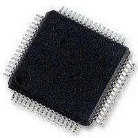
IC MCU 8BIT 32KB FLASH 64LQFP
Manufacturer
Freescale Semiconductor
Series
HCS08r
Specifications of S9S08DN32F1MLH
Core Processor
HCS08
Core Size
8-Bit
Speed
40MHz
Connectivity
I²C, LIN, SCI, SPI
Peripherals
LVD, POR, PWM, WDT
Number Of I /o
53
Program Memory Size
32KB (32K x 8)
Program Memory Type
FLASH
Eeprom Size
1K x 8
Ram Size
1.5K x 8
Voltage - Supply (vcc/vdd)
2.7 V ~ 5.5 V
Data Converters
A/D 16x12b
Oscillator Type
Internal
Operating Temperature
-40°C ~ 125°C
Package / Case
64-LQFP
Processor Series
S08D
Core
HCS08
Data Bus Width
8 bit
Data Ram Size
1.5 KB
Interface Type
SCI, SPI
Maximum Clock Frequency
40 MHz
Number Of Programmable I/os
53
Number Of Timers
8
Maximum Operating Temperature
+ 125 C
Mounting Style
SMD/SMT
3rd Party Development Tools
EWS08
Development Tools By Supplier
DEMO9S08DZ60
Minimum Operating Temperature
- 40 C
On-chip Adc
12 bit, 16 Channel
Lead Free Status / RoHS Status
Lead free / RoHS Compliant
Available stocks
Company
Part Number
Manufacturer
Quantity
Price
Company:

Part Number:
S9S08DN32F1MLH
Manufacturer:
Freescale Semiconductor
Quantity:
10 000


MC9S08DN60 Series Features
8-Bit HCS08 Central Processor Unit (CPU)
On-Chip Memory
Power-Saving Modes
Clock Source Options
System Protection
Development Support
• 40-MHz HCS08 CPU (20-MHz bus)
• HC08 instruction set with added BGND instruction
• Support for up to 32 interrupt/reset sources
• Flash read/program/erase over full operating voltage
• Up to 2K EEPROM in-circuit programmable memory;
• Up to 2K random-access memory (RAM)
• Two very low power stop modes
• Reduced power wait mode
• Very low power real time interrupt for use in run, wait,
• Oscillator (XOSC) — Loop-control Pierce oscillator;
• Multi-purpose Clock Generator (MCG) — PLL and
• Watchdog computer operating properly (COP) reset
• Low-voltage detection with reset or interrupt; selectable
• Illegal opcode detection with reset
• Illegal address detection with reset
• Flash block protect
• Loss-of-lock protection
• Single-wire background debug interface
• On-chip, in-circuit emulation (ICE) with real-time bus
and temperature
— MC9S08DN60 = 60K
— MC9S08DN48 = 48K
— MC9S08DN32 = 32K
— MC9S08DN16 = 16K
8-byte single-page or 4-byte dual-page erase sector;
Program and Erase while executing Flash; Erase abort
and stop
Crystal or ceramic resonator range of 31.25 kHz to
38.4 kHz or 1 MHz to 16 MHz
FLL modes (FLL capable of 1.5% deviation using
internal temperature compensation); Internal reference
clock with trim adjustment (trimmed at factory, with
trim value stored in flash); External reference with
oscillator/resonator options
with option to run from backup dedicated 1-kHz
internal clock source or bus clock
trip points
capture
Peripherals
Input/Output
Package Options
• ADC — 16-channel, 12-bit resolution, 2.5 μs
• ACMPx — Two analog comparators with selectable
• SCI1 — One SCI supporting LIN 2.0 Protocol and SAE
• SPI — Full-duplex or single-wire bidirectional;
• IIC — Up to 100 kbps with maximum bus loading;
• TPMx — One 6-channel (TPM1) and one 2-channel
• RTC — (Real-time counter) 8-bit modulus counter with
• 53 general-purpose input/output (I/O) pins and 1
• 24 interrupt pins with selectable polarity on each pin
• Hysteresis and configurable pull device on all input
• Configurable slew rate and drive strength on all output
• 64-pin low-profile quad flat-pack (LQFP) — 10x10 mm
• 48-pin low-profile quad flat-pack (LQFP) — 7x7 mm
• 32-pin low-profile quad flat-pack (LQFP) — 7x7 mm
conversion time, automatic compare function,
temperature sensor, internal bandgap reference channel
interrupt on rising, falling, or either edge of comparator
output; compare option to fixed internal bandgap
reference voltage
J2602 protocols; Full duplex non-return to zero (NRZ);
Master extended break generation; Slave extended
break detection; Wakeup on active edge
Double-buffered transmit and receive; Master or Slave
mode; MSB-first or LSB-first shifting
Multi-master operation; Programmable slave address;
General Call Address; Interrupt driven byte-by-byte
data transfer
(TPM2); Selectable input capture, output compare, or
buffered edge-aligned PWM on each channel
binary or decimal based prescaler; Real-time clock
capabilities using external crystal and RTC for precise
time base, time-of-day, calendar or task scheduling
functions; Free running on-chip low power oscillator
(1 kHz) for cyclic wake-up without external
components
input-only pin
pins.
pins.
Related parts for S9S08DN32F1MLH
Image
Part Number
Description
Manufacturer
Datasheet
Request
R

Part Number:
Description:
Manufacturer:
Freescale Semiconductor, Inc
Datasheet:
Part Number:
Description:
Manufacturer:
Freescale Semiconductor, Inc
Datasheet:
Part Number:
Description:
Manufacturer:
Freescale Semiconductor, Inc
Datasheet:
Part Number:
Description:
Manufacturer:
Freescale Semiconductor, Inc
Datasheet:
Part Number:
Description:
Manufacturer:
Freescale Semiconductor, Inc
Datasheet:
Part Number:
Description:
Manufacturer:
Freescale Semiconductor, Inc
Datasheet:
Part Number:
Description:
Manufacturer:
Freescale Semiconductor, Inc
Datasheet:
Part Number:
Description:
Manufacturer:
Freescale Semiconductor, Inc
Datasheet:
Part Number:
Description:
Manufacturer:
Freescale Semiconductor, Inc
Datasheet:
Part Number:
Description:
Manufacturer:
Freescale Semiconductor, Inc
Datasheet:
Part Number:
Description:
Manufacturer:
Freescale Semiconductor, Inc
Datasheet:
Part Number:
Description:
Manufacturer:
Freescale Semiconductor, Inc
Datasheet:
Part Number:
Description:
Manufacturer:
Freescale Semiconductor, Inc
Datasheet:
Part Number:
Description:
Manufacturer:
Freescale Semiconductor, Inc
Datasheet:
Part Number:
Description:
Manufacturer:
Freescale Semiconductor, Inc
Datasheet: