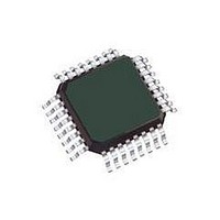
S9S08DZ16F1MLC Freescale Semiconductor, S9S08DZ16F1MLC Datasheet - Page 295

S9S08DZ16F1MLC
Manufacturer Part Number
S9S08DZ16F1MLC
Description
IC MCU 8BIT 16KB FLASH 32LQFP
Manufacturer
Freescale Semiconductor
Series
HCS08r
Datasheet
1.DEMO9S08DZ60.pdf
(416 pages)
Specifications of S9S08DZ16F1MLC
Core Processor
HCS08
Core Size
8-Bit
Speed
40MHz
Connectivity
CAN, I²C, LIN, SCI, SPI
Peripherals
LVD, POR, PWM, WDT
Number Of I /o
25
Program Memory Size
16KB (16K x 8)
Program Memory Type
FLASH
Eeprom Size
512 x 8
Ram Size
1K x 8
Voltage - Supply (vcc/vdd)
2.7 V ~ 5.5 V
Data Converters
A/D 10x12b
Oscillator Type
External
Operating Temperature
-40°C ~ 125°C
Package / Case
32-LQFP
Processor Series
S08D
Core
HCS08
Data Bus Width
8 bit
Data Ram Size
1 KB
Interface Type
I2C, SCI, SPI
Maximum Clock Frequency
40 MHz
Number Of Programmable I/os
26
Operating Supply Voltage
3 V to 5 V
Maximum Operating Temperature
+ 125 C
Mounting Style
SMD/SMT
3rd Party Development Tools
EWS08
Development Tools By Supplier
DEMO9S08DZ60
Minimum Operating Temperature
- 40 C
On-chip Adc
12 bit, 16 Channel
Lead Free Status / RoHS Status
Lead free / RoHS Compliant
Available stocks
Company
Part Number
Manufacturer
Quantity
Price
Company:
Part Number:
S9S08DZ16F1MLC
Manufacturer:
Freescale Semiconductor
Quantity:
10 000
Part Number:
S9S08DZ16F1MLC
Manufacturer:
FREESCALE
Quantity:
20 000
- Current page: 295 of 416
- Download datasheet (5Mb)
14.2.2
This read/write register is used to control various optional features of the SCI system.
Freescale Semiconductor
SCISWAI
SBR[7:0]
Reset
Reset
LOOPS
RSRC
Field
Field
7:0
M
7
6
5
4
W
W
R
R
LOOPS
SBR7
SCI Control Register 1 (SCIxC1)
Baud Rate Modulo Divisor — These 13 bits in SBR[12:0] are referred to collectively as BR, and they set the
modulo divide rate for the SCI baud rate generator. When BR = 0, the SCI baud rate generator is disabled to
reduce supply current. When BR = 1 to 8191, the SCI baud rate = BUSCLK/(16×BR). See also BR bits in
Table
Loop Mode Select — Selects between loop back modes and normal 2-pin full-duplex modes. When
LOOPS = 1, the transmitter output is internally connected to the receiver input.
0 Normal operation — RxD and TxD use separate pins.
1 Loop mode or single-wire mode where transmitter outputs are internally connected to receiver input. (See
SCI Stops in Wait Mode
0 SCI clocks continue to run in wait mode so the SCI can be the source of an interrupt that wakes up the CPU.
1 SCI clocks freeze while CPU is in wait mode.
Receiver Source Select — This bit has no meaning or effect unless the LOOPS bit is set to 1. When
LOOPS = 1, the receiver input is internally connected to the TxD pin and RSRC determines whether this
connection is also connected to the transmitter output.
0 Provided LOOPS = 1, RSRC = 0 selects internal loop back mode and the SCI does not use the RxD pins.
1 Single-wire SCI mode where the TxD pin is connected to the transmitter output and receiver input.
9-Bit or 8-Bit Mode Select
0 Normal — start + 8 data bits (LSB first) + stop.
1 Receiver and transmitter use 9-bit data characters
0
0
7
7
RSRC
start + 8 data bits (LSB first) + 9th data bit + stop.
14-2.
bit.) RxD pin is not used by SCI.
SCISWAI
SBR6
0
0
6
6
Figure 14-5. SCI Baud Rate Register (SCIxBDL)
Figure 14-6. SCI Control Register 1 (SCIxC1)
Table 14-3. SCIxBDL Field Descriptions
Table 14-4. SCIxC1 Field Descriptions
MC9S08DZ60 Series Data Sheet, Rev. 4
RSRC
SBR5
0
0
5
5
SBR4
M
0
0
4
4
Description
Description
WAKE
SBR3
Chapter 14 Serial Communications Interface (S08SCIV4)
3
0
3
0
SBR2
ILT
1
0
2
2
SBR1
PE
0
0
1
1
SBR0
PT
0
0
0
0
295
Related parts for S9S08DZ16F1MLC
Image
Part Number
Description
Manufacturer
Datasheet
Request
R
Part Number:
Description:
Manufacturer:
Freescale Semiconductor, Inc
Datasheet:
Part Number:
Description:
Manufacturer:
Freescale Semiconductor, Inc
Datasheet:
Part Number:
Description:
Manufacturer:
Freescale Semiconductor, Inc
Datasheet:
Part Number:
Description:
Manufacturer:
Freescale Semiconductor, Inc
Datasheet:
Part Number:
Description:
Manufacturer:
Freescale Semiconductor, Inc
Datasheet:
Part Number:
Description:
Manufacturer:
Freescale Semiconductor, Inc
Datasheet:
Part Number:
Description:
Manufacturer:
Freescale Semiconductor, Inc
Datasheet:
Part Number:
Description:
Manufacturer:
Freescale Semiconductor, Inc
Datasheet:
Part Number:
Description:
Manufacturer:
Freescale Semiconductor, Inc
Datasheet:
Part Number:
Description:
Manufacturer:
Freescale Semiconductor, Inc
Datasheet:
Part Number:
Description:
Manufacturer:
Freescale Semiconductor, Inc
Datasheet:
Part Number:
Description:
Manufacturer:
Freescale Semiconductor, Inc
Datasheet:
Part Number:
Description:
Manufacturer:
Freescale Semiconductor, Inc
Datasheet:
Part Number:
Description:
Manufacturer:
Freescale Semiconductor, Inc
Datasheet:
Part Number:
Description:
Manufacturer:
Freescale Semiconductor, Inc
Datasheet:


