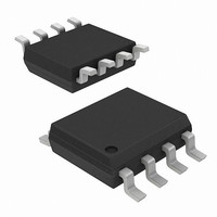
DMS3019SSD-13 Diodes Inc, DMS3019SSD-13 Datasheet - Page 8

DMS3019SSD-13
Manufacturer Part Number
DMS3019SSD-13
Description
MOSFET 2N-CH 30V 7A/5.7A SO8
Manufacturer
Diodes Inc
Datasheet
1.DMS3019SSD-13.pdf
(10 pages)
Specifications of DMS3019SSD-13
Fet Type
2 N-Channel (Dual)
Fet Feature
Logic Level Gate
Rds On (max) @ Id, Vgs
15 mOhm @ 9A, 10V
Drain To Source Voltage (vdss)
30V
Current - Continuous Drain (id) @ 25° C
7A, 5.7A
Vgs(th) (max) @ Id
2.4V @ 250µA
Gate Charge (qg) @ Vgs
42nC @ 10V
Input Capacitance (ciss) @ Vds
1932pF @ 15V
Power - Max
1.19W
Mounting Type
Surface Mount
Package / Case
8-SOIC (0.154", 3.90mm Width)
Configuration
Dual
Transistor Polarity
N-Channel
Resistance Drain-source Rds (on)
10 mOhms
Gate Charge Qg
42 nC
Forward Transconductance Gfs (max / Min)
5 S
Drain-source Breakdown Voltage
30 V
Gate-source Breakdown Voltage
20 V
Continuous Drain Current
7 A
Power Dissipation
1.19 W
Maximum Operating Temperature
+ 150 C
Mounting Style
SMD/SMT
Minimum Operating Temperature
- 55 C
Lead Free Status / RoHS Status
Lead free / RoHS Compliant
Other names
DMS3019SSD-13DITR
DMS3019SSD
Document number: DS35053 Rev. 2 - 2
1,000
100
10
10
8
6
4
2
0
0
0
0.001
0.01
Fig. 22 Gate-Charge Characteristics
2
V , DRAIN-SOURCE VOLTAGE (V)
0.1
5
Q , TOTAL GATE CHARGE (nC)
DS
0.00001
1
Fig. 20 Typical Total Capacitance
g
C
D = 0.1
D = 0.02
D = 0.01
D = 0.005
D = 0.05
D = 0.7
V
D = 0.5
D = 0.3
rss
I = 10A
D = Single Pulse
DS
D
C
4
10
oss
= 15V
C
iss
0.0001
6
15
8
20
0.001
f = 1MHz
10
25
Fig. 23 Transient Thermal Response
t , PULSE DURATION TIME (s)
0.01
1
12
30
www.diodes.com
D = 0.9
0.1
8 of 10
10,000
1,000
100
10
1
0
1
V , DRAIN-SOURCE VOLTAGE (V)
5
DS
Fig. 21 Typical Leakage Current
10
P(pk)
vs. Drain-Source Voltage
Duty Cycle, D = t /t
T - T = P * R
10
R
J
θJA
R
θ
JA
t
(t) = r(t) *
A
1
t
= 113°C/W
2
100
15
θ
R
JA
1 2
θ
JA
(t)
DMS3019SSD
20
T = 150°C
1,000
A
T = 125°C
T = 25°C
A
A
T = 85°C
A
25
© Diodes Incorporated
October 2010
30


