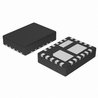
NUS6160MNTWG ON Semiconductor, NUS6160MNTWG Datasheet

NUS6160MNTWG
Specifications of NUS6160MNTWG
Related parts for NUS6160MNTWG
NUS6160MNTWG Summary of contents
Page 1
... G = Pb−Free Package (Note: Microdot may be in either location) ORDERING INFORMATION Device Package Shipping NUS6160MNTWG QFN22 3000 / (Pb−Free) Tape & Reel †For information on tape and reel specifications, including part orientation and tape sizes, please refer to our Tape and Reel Packaging Specification Brochure, BRD8011/D ...
Page 2
Out N/C Gate1 Drain1 FET Drain1 Drain1 Wall Adaptor IN EN NUS6160 18 Figure 2. Typical Charging Solution 18 N/C FET REG SW Drain2 Drain1 11 (Top View) Figure 1. Pinout V bat 15 1 ...
Page 3
MAXIMUM RATINGS (T = 25°C, unless otherwise stated) J Rating V to Ground IN OUT, EN, FLAG Pins Voltage to Ground Maximum Current from (PMOS) IN OUT Drain−to−Source Voltage Gate−to−Source Voltage Continuous Drain Current, Steady State Pulsed ...
Page 4
PIN DESCRIPTION Pin Name 1 Out This pin is the output of the internal OVP chip. It must be connected to the source of the upper FET (Pin 8). 3 Gate FET This pin is the gate of the upper ...
Page 5
OVP ELECTRICAL CHARACTERISTICS (Min/Max limits values (−40°C < T < +85°C) and V A Characteristic Symbol Input Voltage Range Undervoltage Lockout UVLO Threshold Undervoltage Lockout UVLO Hysteresis Overvoltage Lockout Threshold OVLO Overvoltage Lockout Hysteresis OVLO V versus V Dropout V ...
Page 6
MOSFET ELECTRICAL CHARACTERISTICS FET ) REG Characteristic OFF CHARACTERISTICS Drain−to−Source Breakdown Voltage Drain−to−Source Breakdown Voltage Temperature Coefficient Zero Gate Voltage Drain Current Gate−to−Source Leakage Current ON CHARACTERISTICS (Note 2) Gate Threshold Voltage Gate Threshold Temperature Coefficient Drain−to−Source On Resistance Forward ...
Page 7
UVLO 0 out t start FLAG 1.2 V Figure 3. Start Up Sequence EN 1 dis V out 0 − DS(on) FLAG Figure 5. Disable ...
Page 8
TYPICAL OPERATING CHARACTERISTICS Figure 9. Startup V = Ch1 Ch3 in out Figure 11. Output Turn Off Time V = Ch1 Ch2 in out Figure 13. Disable Time EN = Ch1 Ch2, FLAG = ...
Page 9
TYPICAL OPERATING CHARACTERISTICS Figure 15. Direct Output Short Circuit 180 160 140 120 100 80 25° Figure 17. Supply Quiescent Current vs. V 450 400 350 300 250 200 150 100 50 0 −50 ...
Page 10
TYPICAL PERFORMANCE CURVES − −2 −V , DRAIN−TO−SOURCE VOLTAGE (VOLTS) DS Figure 18. On−Region Characteristics 0.2 0.18 ...
Page 11
TYPICAL PERFORMANCE CURVES 1000 900 800 700 600 500 400 300 200 100 C rss −V − GATE−TO−SOURCE OR DRAIN−TO−SOURCE VOLTAGE (VOLTS) Figure 23. Capacitance Variation 1000 V = −10 ...
Page 12
Operational Description The NUS6160 provides overvoltage protection for positive voltages P−Channel FET protects the load connected on the V pin, against positive overvoltage out conditions. The Output follows the V BUS threshold is reached. Undervoltage ...
Page 13
... C e 22X 0.52 *For additional information on our Pb−Free strategy and soldering details, please download the ON Semiconductor Soldering and Mounting Techniques Reference Manual, SOLDERRM/D. N. American Technical Support: 800−282−9855 Toll Free USA/Canada Europe, Middle East and Africa Technical Support: Phone: 421 33 790 2910 Japan Customer Focus Center Phone: 81− ...


