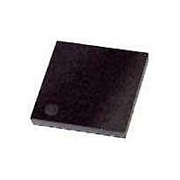
XR18W753IL48-F Exar Corporation, XR18W753IL48-F Datasheet - Page 5

XR18W753IL48-F
Manufacturer Part Number
XR18W753IL48-F
Description
IC RF TXRX 868-956MHZ 48QFN
Manufacturer
Exar Corporation
Type
RF Receiversr
Series
-r
Datasheet
1.XR18W753IL48-F.pdf
(27 pages)
Specifications of XR18W753IL48-F
Package / Case
48-VFQFN Exposed Pad
Frequency
868MHz ~ 954MHz
Data Rate - Maximum
250kbps
Modulation Or Protocol
DSSS
Applications
ISM
Power - Output
0dBm
Sensitivity
-94dBm
Voltage - Supply
2.2 V ~ 3.6 V
Current - Receiving
19mA
Current - Transmitting
22mA
Data Interface
PCB, Surface Mount
Antenna Connector
PCB, Surface Mount
Operating Temperature
-40°C ~ 85°C
Operating Frequency
100 KHz, 400 KHz
Operating Supply Voltage
2.2 V to 3.6 V
Maximum Operating Temperature
+ 85 C
Minimum Operating Temperature
- 40 C
Mounting Style
SMD/SMT
Noise Figure
12 dB
Supply Current
0.5 mA, 1.7 mA, 19 mA, 22 mA
Data Rate
250Kbps
Rf Ic Case Style
QFN
No. Of Pins
48
Supply Voltage Range
2.97V To 3.63V
Operating Temperature Range
-40°C To +85°C
Memory Size
-
Lead Free Status / RoHS Status
Lead free / RoHS Compliant
Lead Free Status / RoHS Status
Lead free / RoHS Compliant, Lead free / RoHS Compliant
Available stocks
Company
Part Number
Manufacturer
Quantity
Price
Part Number:
XR18W753IL48-F
Manufacturer:
EXAR/艾科嘉
Quantity:
20 000
REV. 1.0.0
Pin type: I=Input, O=Output, I/O= Input/output, OD=Output Open Drain.
MODEM_RESET
VREG_CLK_EN
DVDD_OUT
AVDD_OUT
CLK_OUT+
CLK_OUT-
PADDLE
AVDD19
AVDD19
AVDD19
AVDD19
TEST2
XTAL1
XTAL2
AGND
DVDD
AVDD
N
A2
A3
AME
P
31
32
33
34
35
36
37
38
39
40
41
42
43
44
45
46
47
48
49
IN
Power O
Power O
Digital O
Digital O
Analog I
Analog I
Digital I
Digital I
Digital I
Power I
Ground
Power I
Power I
Power I
Power I
Power I
Ground
Digital I
Digital I
T
YPE
Factory Test Mode. For normal operation, this pin should be connected
to GND.
I2C Address bit-2
I2C Address bit-3. This address line should be connected to GND.
16 MHz LVDS digital clock outputs. Connect pin 35 to ground for
CMOS clock output.
Digital modem reset (active high, level sensitive).
Voltage Regulator and crystal oscillator enable (active high, level sensi-
tive)
VDD (1.9V ± 0.1V) for crystal oscillator and clock divider.
16MHz crystal input or external clock input. Based on typical PCB stray
capacitance, a 27 pF capacitor to GND is recommended.
Crystal output, 27 pF capacitor to GND is recommended. If an external
clock is used at XTAL1, this input should be left unconnected.
Ground for crystal oscillator and buffers.
Decoupling pin for digital VDD, 10 nF capacitor to GND recommended.
Digital Power Supply, DVDD = 2.2 - 3.6V. DVDD and AVDD should use
the same power supply. 100nF capacitor to GND recommended.
Analog Power Supply, AVDD = 2.2 - 3.6V. DVDD and AVDD should use
the same power supply. 100nF capacitor to GND recommended.
1.9V stabilized analog VDD output. This output should be connected to
all AVDD19 pins. 1uF ceramic capacitor to GND recommended.
Analog VDD (1.9V ± 0.1V) for ADC and DAC.
Analog VDD (1.9V ± 0.1V) for ADC.
Analog VDD (1.9V ± 0.1V) for IF strip, TX mixers and both I/Q dividers.
The center pad on the backside of the 48-QFN package is metallic and
is not electrically connected to anything inside the device. It must be
soldered on to the PCB and may be optionally connected to GND on the
PCB. The thermal pad size on the PCB should be the approximate size
of this center pad and should be solder mask defined. The solder mask
opening should be at least 0.0025" inwards from the edge of the PCB
thermal pad.
SINGLE CHIP 868MHZ TO 956MHZ RF TRANSCEIVER
5
D
ESCRIPTION
XR18W753


