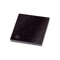
XR18W753IL48-F Exar Corporation, XR18W753IL48-F Datasheet - Page 12

XR18W753IL48-F
Manufacturer Part Number
XR18W753IL48-F
Description
IC RF TXRX 868-956MHZ 48QFN
Manufacturer
Exar Corporation
Type
RF Receiversr
Series
-r
Datasheet
1.XR18W753IL48-F.pdf
(27 pages)
Specifications of XR18W753IL48-F
Package / Case
48-VFQFN Exposed Pad
Frequency
868MHz ~ 954MHz
Data Rate - Maximum
250kbps
Modulation Or Protocol
DSSS
Applications
ISM
Power - Output
0dBm
Sensitivity
-94dBm
Voltage - Supply
2.2 V ~ 3.6 V
Current - Receiving
19mA
Current - Transmitting
22mA
Data Interface
PCB, Surface Mount
Antenna Connector
PCB, Surface Mount
Operating Temperature
-40°C ~ 85°C
Operating Frequency
100 KHz, 400 KHz
Operating Supply Voltage
2.2 V to 3.6 V
Maximum Operating Temperature
+ 85 C
Minimum Operating Temperature
- 40 C
Mounting Style
SMD/SMT
Noise Figure
12 dB
Supply Current
0.5 mA, 1.7 mA, 19 mA, 22 mA
Data Rate
250Kbps
Rf Ic Case Style
QFN
No. Of Pins
48
Supply Voltage Range
2.97V To 3.63V
Operating Temperature Range
-40°C To +85°C
Memory Size
-
Lead Free Status / RoHS Status
Lead free / RoHS Compliant
Lead Free Status / RoHS Status
Lead free / RoHS Compliant, Lead free / RoHS Compliant
Available stocks
Company
Part Number
Manufacturer
Quantity
Price
Part Number:
XR18W753IL48-F
Manufacturer:
EXAR/艾科嘉
Quantity:
20 000
XR18W753
SINGLE CHIP 868MHZ TO 956MHZ RF TRANSCEIVER
3.2 DETAILED REGISTERS DESCRIPTIONS
A
0x00
0x01
0x02
0x03
0x04
DDRESS
REGISTER NAME
READ_SUBADDRESS
RX_FIFO
TX_FIFO
FIFO_CONTROL
INT_MASKING
DESCRIPTION
b[7:0]
To ease reading via I2C, the data of READ_SUBADDRESS is a
pointer to the first address in the I2C memory map. If the master
wants to read the content of register e.g. 0x2E, the master first
need to write 0x2E to READ_SUBADDRESS.
b[7:0]
To retrieve data from the RX Data Buffer, the master must read
from this register. All entries of the RX Data Buffer are mapped to
this register, offering a FIFO mechanism.
b[7:0]
To put data into the TX Data Buffer, the master must write to this
register. All entries of the TX Data Buffer are mapped to this regis-
ter, offering a FIFO mechanism.
b[2:0] = 001 --> reset RX_FIFO read address
b[2:0] = 010 --> reset RX_FIFO write address
b[2:0] = 011 --> reset TX_FIFO read address
b[2:0] = 100 --> reset TX_FIFO write address
b[2:0] = 101 --> reset RX_FIFO read address
b[2:0] = 110 --> reset RX_FIFO write address
b[2:0] = 001 --> reset RX_FIFO read address
b[2:0] = 111 --> reset all RX and TX FIFO addresses
b[7:3] not used
Via this register, the internal FIFO read and write pointers of the TX
Data Buffer and the RX Data Buffer can be set to 0X00. The con-
tent of the Data Buffers is unaffected by resetting the pointers.
b[0] = 0 --> pck_tx_ready interrupt disabled
b[0] = 1 --> pck_tx_ready interrupt enabled
b[1] = 0 --> pck_received interrupt disabled
b[1] = 1 --> pck_received interrupt enabled
b[2] = 0 --> cca_ed_ready interrupt disabled
b[2] = 1 --> cca_ed_ready interrupt enabled
b[3] = 0 --> plme_ready interrupt disabled
b[3] = 1 --> plme_ready interrupt enabled
b[7:4] not used
Via this register, the internal modem interrupts can be enabled or
disabled. PLME_ready is enabled at start-up; after reset, a
PLME_ready is generated.
12
REV. 1.0.0
T
R/W
R/W
R/W
YPE
W
R


